
Sobre SHENZHEN JERICO MULTILAYER PCB CO., LTD
We are capable of manufacturing rigid PCBs from 1‑18 layers, including heavy copper PCB, HDI with buried & blind vias, high‑frequency board, metal‑core PCB and other special‑material boards. Our products serve industries of communication, automotive electronics, industrial control, smart home, consumer 3C electronics, medical equipment and power energy. We have established stable cooperation with well‑known brands such as Xiaomi, ZTE, Ecovacs, BDstar, Changhong and Legrand.
Equipped with complete automatic production lines and reliability laboratory, we strictly implement IPC, UL and IATF16949 specifications. 7×24‑hour technical support and order service are available for global.
Strength & Capabilities
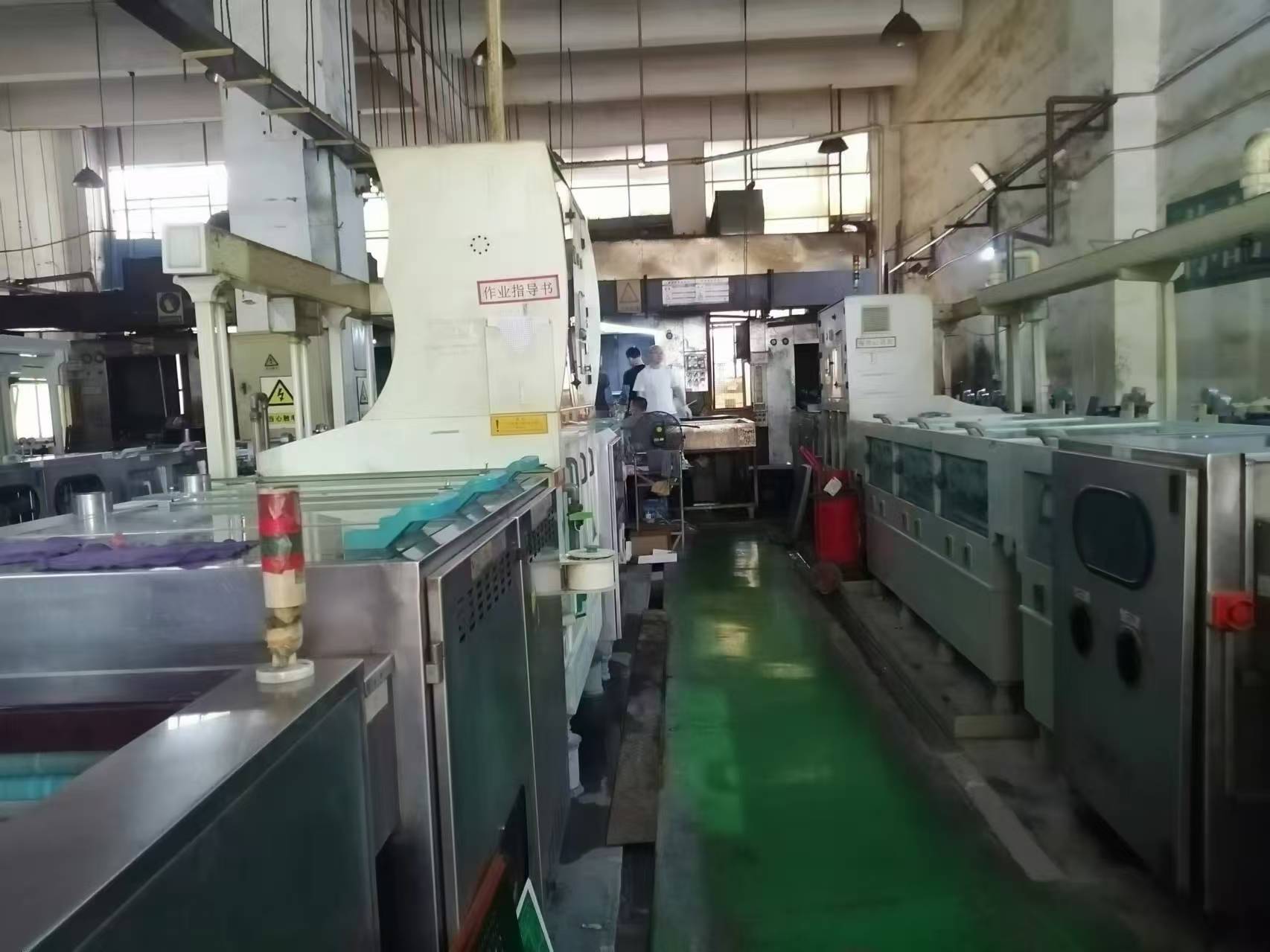
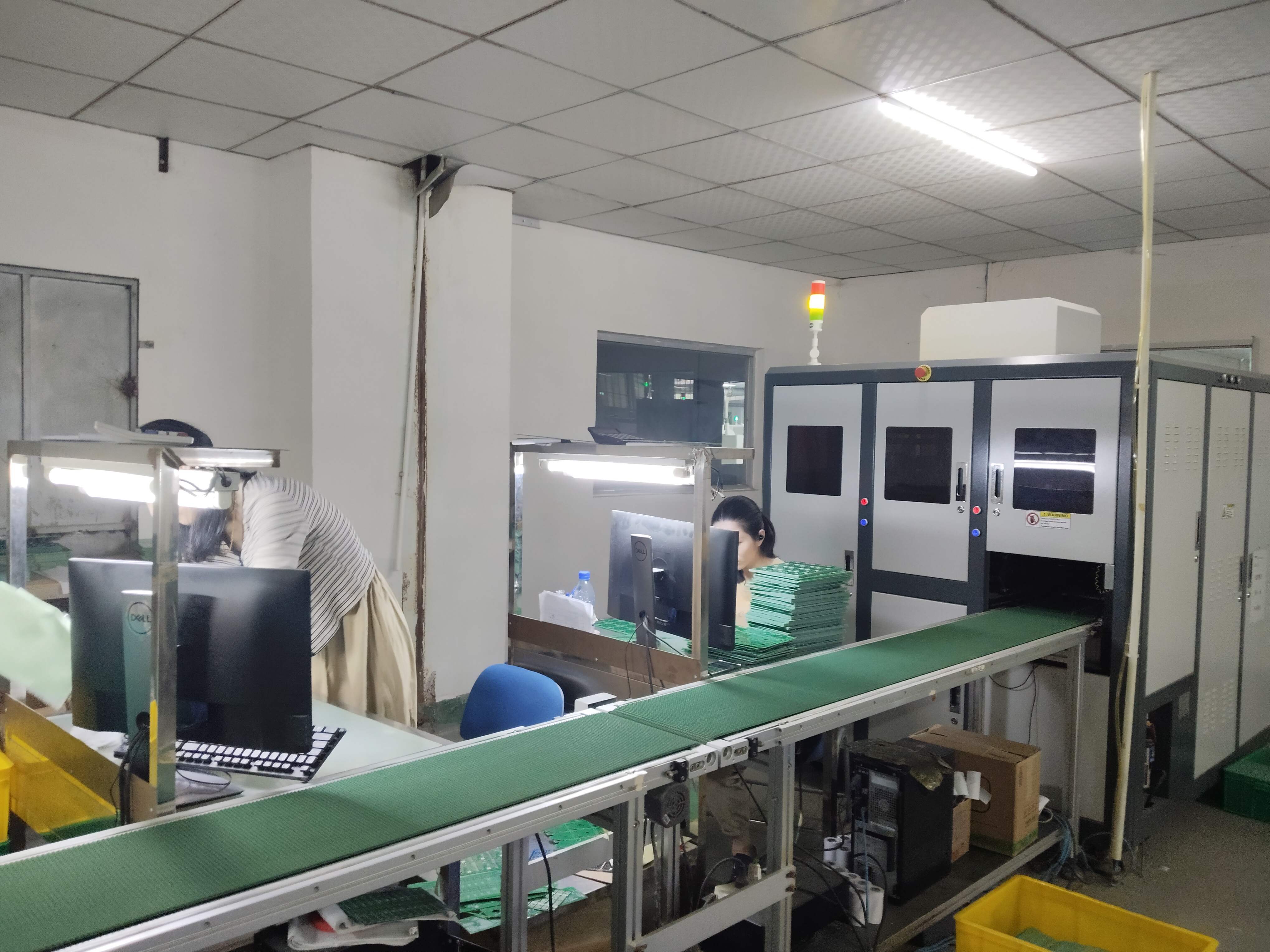
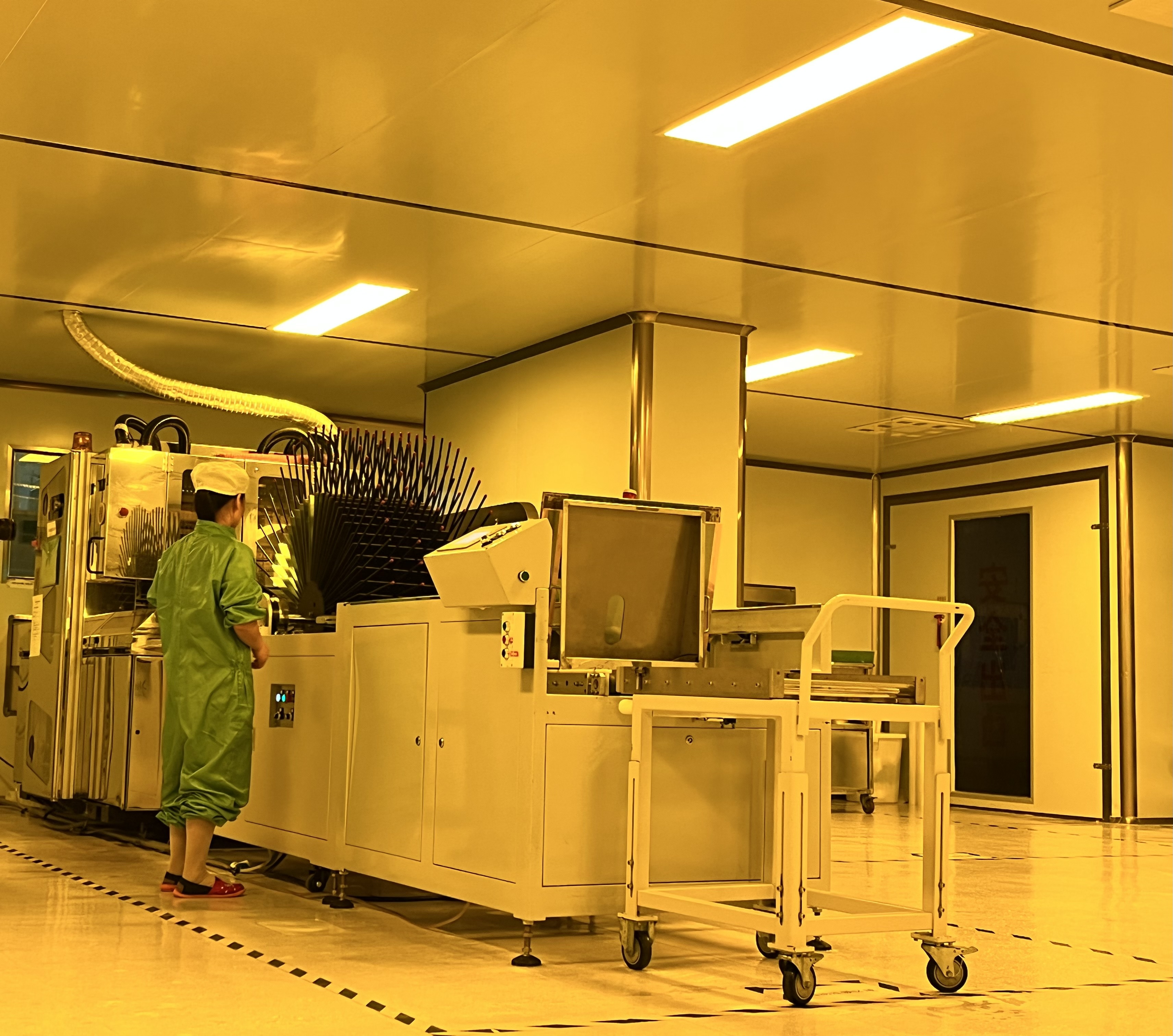
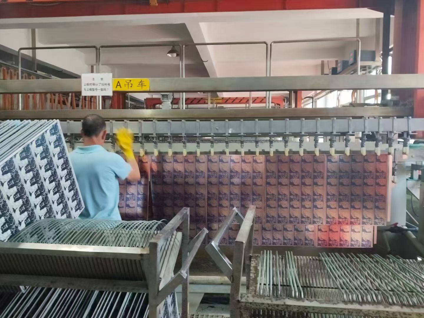
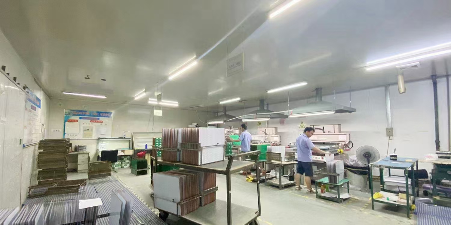
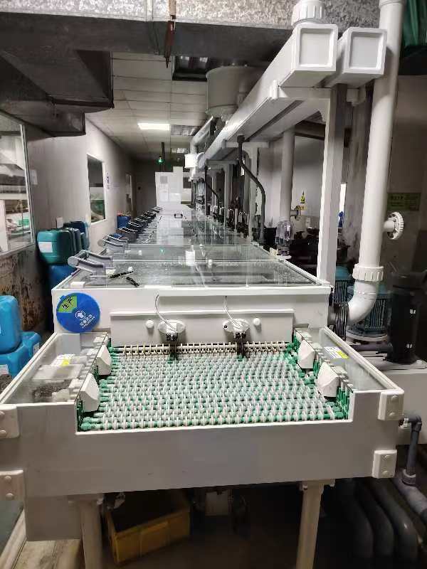
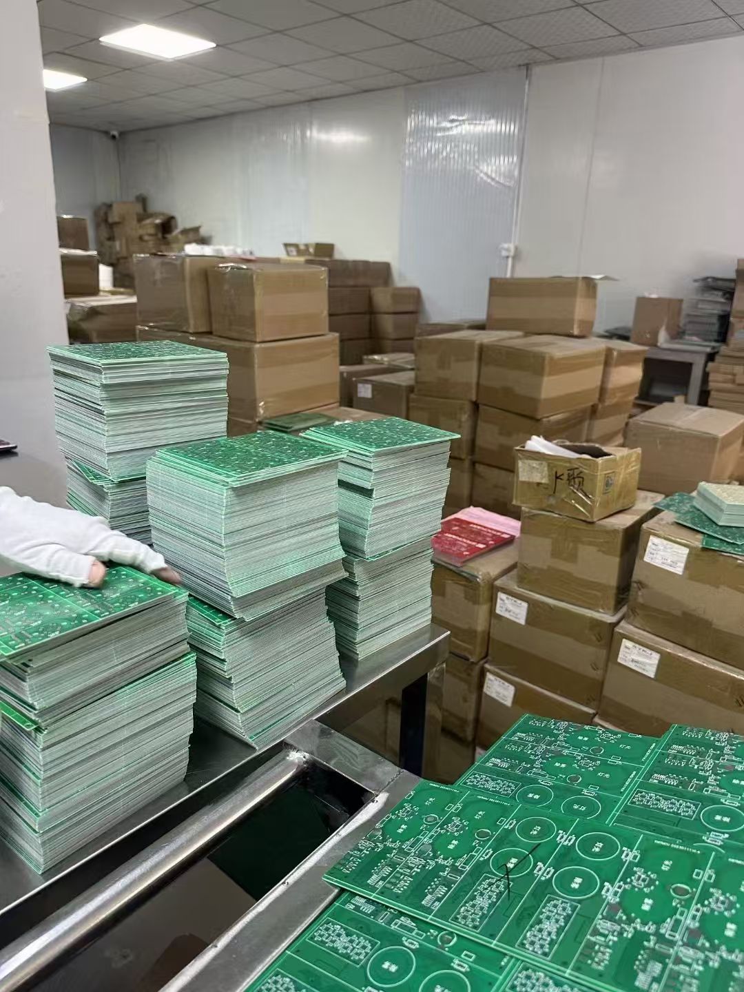
Manufacturing Scale: We own Wuping production base in Fujian with 20,000㎡ plant area and complete waste‑water treatment facilities. Monthly capacity ranges from 50,000 to 70,000 square meters. Full‑set automatic production & testing facilities are deployed, including LDI direct imaging exposure, vacuum laminator, AOI inspection, X‑RAY, flying‑probe tester and independent reliability lab for salt‑spray, high‑voltage and metallographic tests.
Technical Expertise: Mass‑production capability for 1‑18 layer rigid PCBs, covering heavy‑copper board, HDI with blind & buried vias, high‑frequency board and metal‑base PCB. Minimum trace width & spacing down to 3/2.8mil; impedance tolerance ±10%; full range of surface finishes including ENIG, ENEPIG, selective gold plating, OSP, Immersion Tin/Silver, HASL etc.
Quality Control: Closed‑loop quality management from IQC incoming check, IPQC in‑process control, AOI full inspection, FQC final inspection to lab reliability validation. Production complies with IPC‑A‑600H, IPC‑6012, UL‑796 and IATF16949 standards. Customer complaint response within 24 hours; corrective & preventive report available within 72 hours.
Customer Service: 7×24‑hour support for technical consultation, order follow‑up and production coordination. Fast‑turn prototype service and stable mass‑production delivery for global customers. Full compliance documents such as RoHS, REACH material declarations are available upon request.
Certifications & Honors
ISO 9001 Quality Management System
ISO 14001 Environmental Management System
IATF 16949:2016 Automotive Quality Management System
UL Recognized (File No. E519316)
CQC China Compulsory Product Certification
National High‑tech Enterprise Certificate
RoHS, REACH & SGS compliance test reports
Alibaba Verified On‑site Audited Supplier
Nossos produtos
Ver todos os produtos → →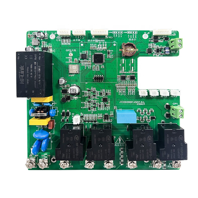
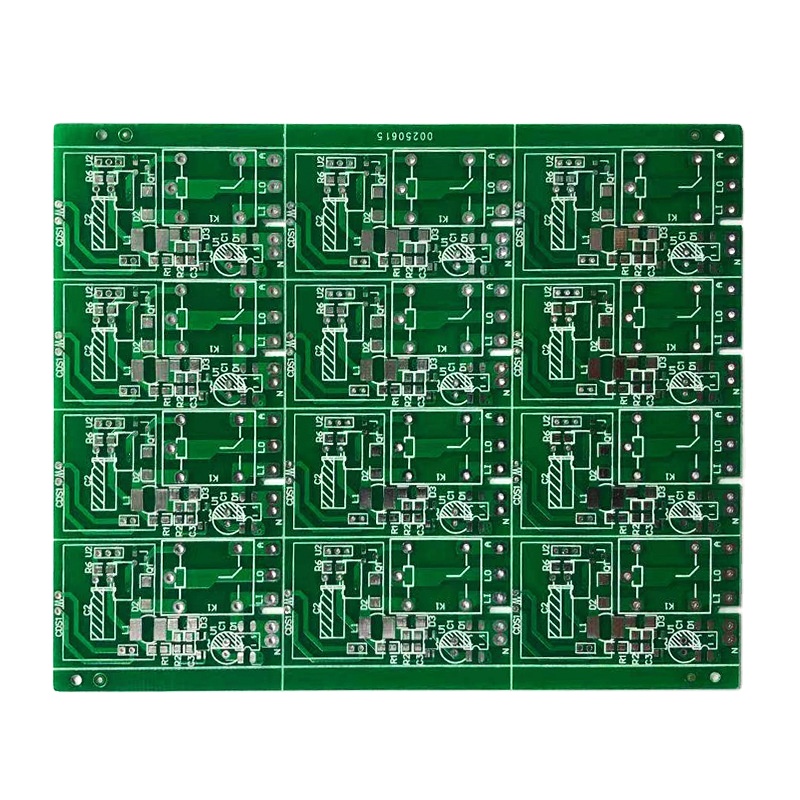
PCBA
Modelo: PCBA-999
Parâmetros: Product Name: PCB-999
Layer Number:4 Layers
Surface Finishing: HASL Lead-Free
PCBA Service: SMD SMT DIP Component Assembly
Certificate:UL/ TS16949/ RoHS/ Reach/ CQC
O/S Test Method: Fixture E-test Or Fly-probe E-test According To Order Quantity
MOQ:1 PCS
Solder Mask Color: Green
Silkscreen Color: White
Package: Vacuum Package
Type: Multilayer PCB
Solder Mask: Green
Place of Origin: CN; GUA
Brand Name: JRC/ JERICO
Base Material: FR-4
Copper Thickness:1oz
Board Thickness:1.2mm
Min. Hole Size: 0.2 mm
Min. Line Width:3mil
Min. Line Spacing:3mil
Board Size:1.6mm
PCB
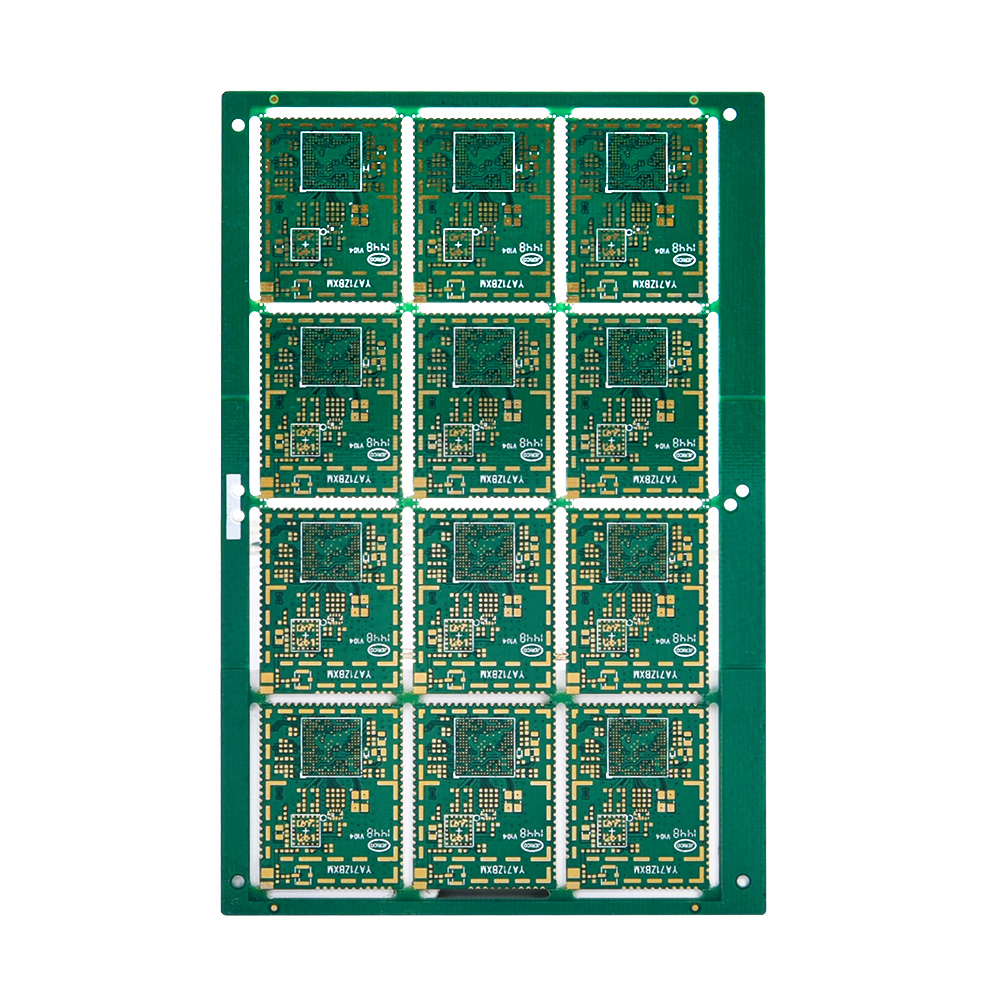
Modelo: PCB-10
Parâmetros: Product Name: PCB-10
Layer Number:4 Layers
Surface Finishing: HASL Lead-Free
PCBA Service: SMD SMT DIP Component Assembly
Certificate:UL/ TS16949/ RoHS/ Reach/ CQC
O/S Test Method: Fixture E-test Or Fly-probe E-test According To Order Quantity
MOQ:1 PCS
Solder Mask Color: Green
Silkscreen Color: White
Package: Vacuum Package
Type: Multilayer PCB
Solder Mask: Green
Place of Origin: CN; GUA
Brand Name: JRC/ JERICO
Base Material: FR-4
Copper Thickness:1oz
Board Thickness:1.0mm/ 1.2mm/1.6mm/ Customized
Min. Hole Size: 0.2 mm
Min. Line Width:3mil
Min. Line Spacing:3mil
Board Size:1.6mm
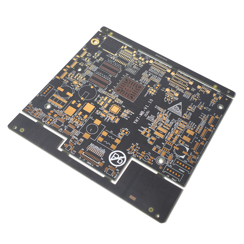
PCB
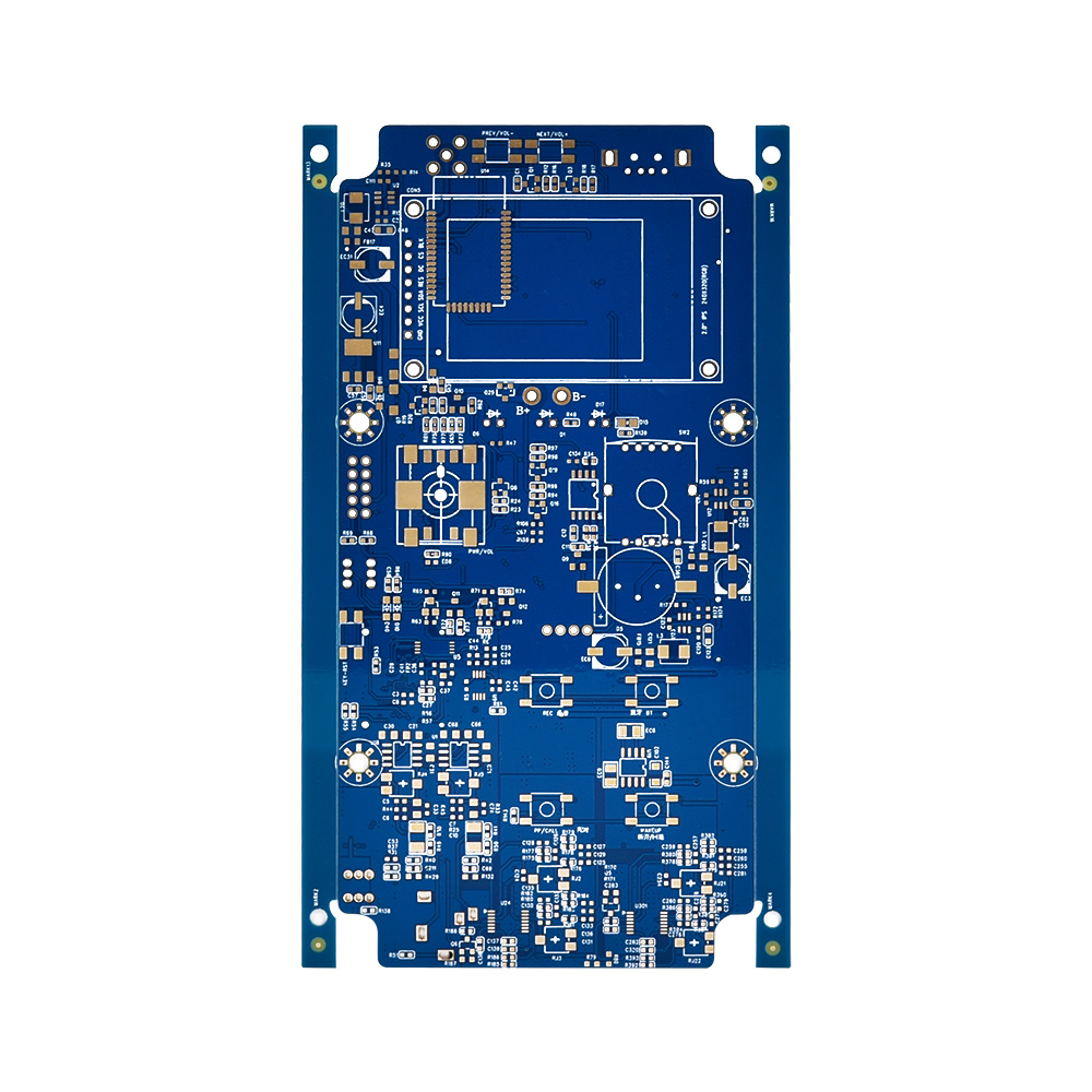
Modelo: PCB-54
Parâmetros: Product Name: PCB-54
Surface Finishing: ENIG
Layer Number:6 Layers
Material:FR-4
Finished Copper Thickness: 2 oz
Min. Hole Size: 0.15 mm
Min. Line Spacing:3mil
MOQ:1 PCS
Color:OEM
Package: Vacuum Package
Material:FR-4
Place of Origin: CN; GUA
Brand Name: JRC/ JERICO
Base Material: FR-4
Copper Thickness:1oz
Board Thickness:1.6mm
Min. Hole Size: 0.15 mm
Min. Line Width:3mil
Min. Line Spacing:3mil
Solder mask color: Blue
Board Size: OEM
PCB
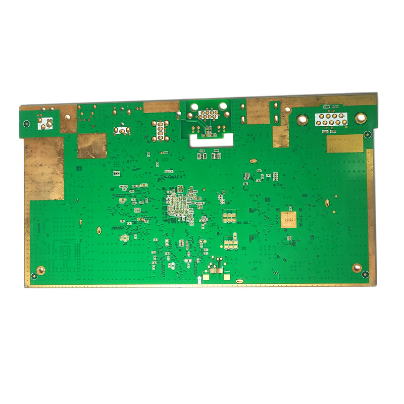
Modelo: PCB-55
Parâmetros: Product Name: PCB-55
Surface Finishing: ENIG
Layer Number:6 Layers
Material:FR-4
Finished Copper Thickness: 1 oz
Min. Hole Size: 0.15 mm
Min. Line Spacing:3mil
MOQ:1 PCS
Color:OEM
Package: Vacuum Package
Material:FR-4
Place of Origin: CN; GUA
Brand Name: JRC/ JERICO
Base Material: FR-4
Copper Thickness:1oz
Board Thickness:1.6mm
Min. Hole Size: 0.15 mm
Min. Line Width:3mil
Min. Line Spacing:3mil
Solder mask color: Green
Board Size: OEM
PCB
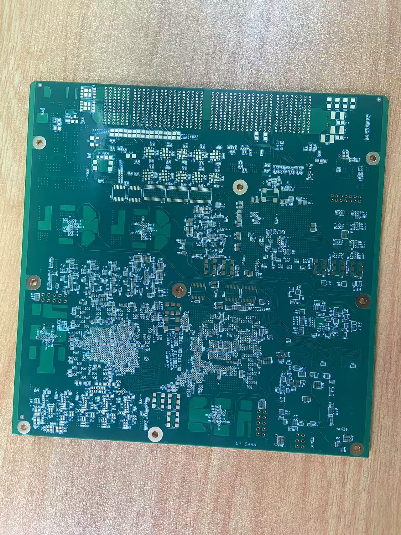
Modelo: PCB-56
Parâmetros: Product Name: PCBA
Surface Finishing: ENIG
Layer Number: 4 Layers
Material:FR-4
Finished Copper Thickness: 1 oz
Min. Hole Size: 0.15 mm
Min. Line Spacing:3mil
Color:Black
Package: Vacuum Package
Material:FR-4
Place of Origin: CN; GUA
Brand Name: JRC/ JERICO
Base Material: FR-4
Copper Thickness:1oz
Board Thickness:1.0mm
Min. Hole Size: 0.15 mm
Min. Line Width:3mil
Min. Line Spacing:3mil
Surface Finishing: ENIG
Board Size: OEM
HDI
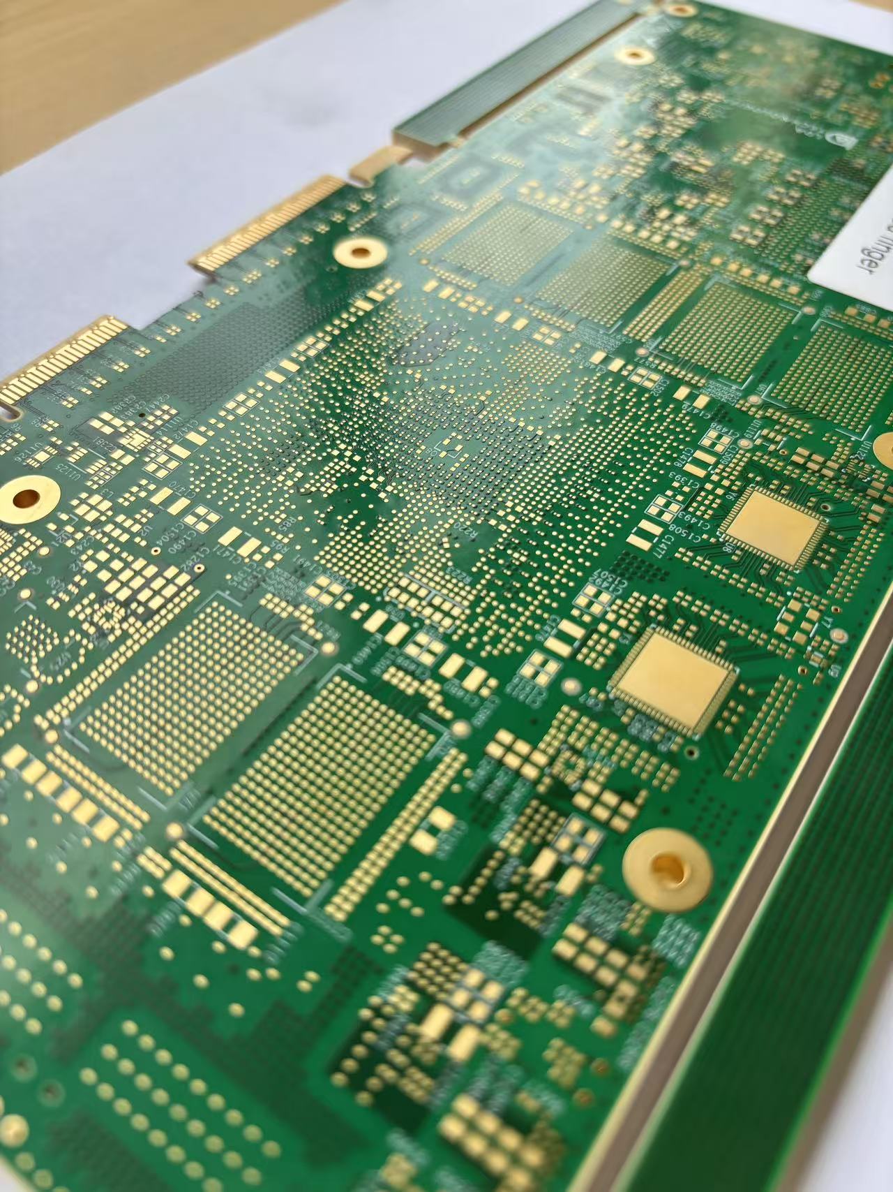
Modelo: TU-883 hsd hdi 18L
Parâmetros: Layer:18‑Layer, 2‑step HDI
Stack‑up:2+14+2
Base Material: High‑Tg FR‑4, Tg≥170℃
Finished Board Thickness:2.40mm ±0.10mm
Outer copper thickness:2oz(70μm)
Inner copper thickness:2oz(70μm)
Min BGA pitch: 0.5 mm
Controlled impedance:Differential 100Ω±8%, Single‑ended 50Ω±10% for PCIe high‑speed signal
Solder mask: Green
Silkscreen:White
Surface treatment: ENIG 1U"
Gold finger: Hard gold plating 30U"
Step depth: 0.8 mm
PTH & Laser blind vias
Electrical Test:100% Flying‑probe test
X‑ray inspection for BGA microvias
Compliance:IPC‑A‑6012 Class3, UL94 V‑0
Panel: Single-piece delivery
HDI
Modelo: M7
Parâmetros: Layer:32‑Layer, 3‑step HDI
Stack‑up:4+24+4
Base Material: High‑Tg FR‑4, Tg≥180℃
Finished Board Thickness:3.20mm ±0.10mm
Outer copper thickness:2oz(70μm)
Inner copper thickness:2oz(70μm)
Min BGA pitch: 0.4 mm
Controlled impedance:Differential 100Ω±8%, Single‑ended 50Ω±10% for PCIe high‑speed signal
Solder mask: Green
Silkscreen:White
Surface treatment: ENIG 1U"
Gold finger: Hard gold plating 30U"
Step depth: 0.8 mm
PTH & Laser blind vias
Electrical Test:100% Flying‑probe test
X‑ray inspection for BGA microvias
Compliance:IPC‑A‑6012 Class3, UL94 V‑0
Panel: Single-piece delivery
Galeria da empresa
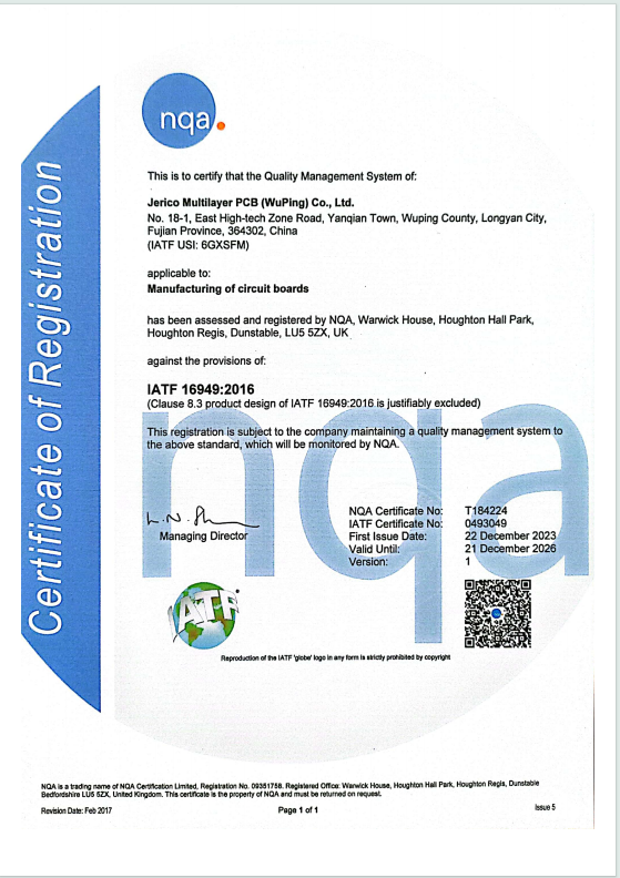
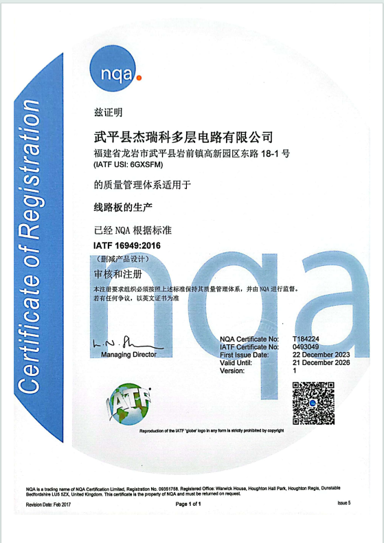
Certificações e prêmios
Histórias de sucesso
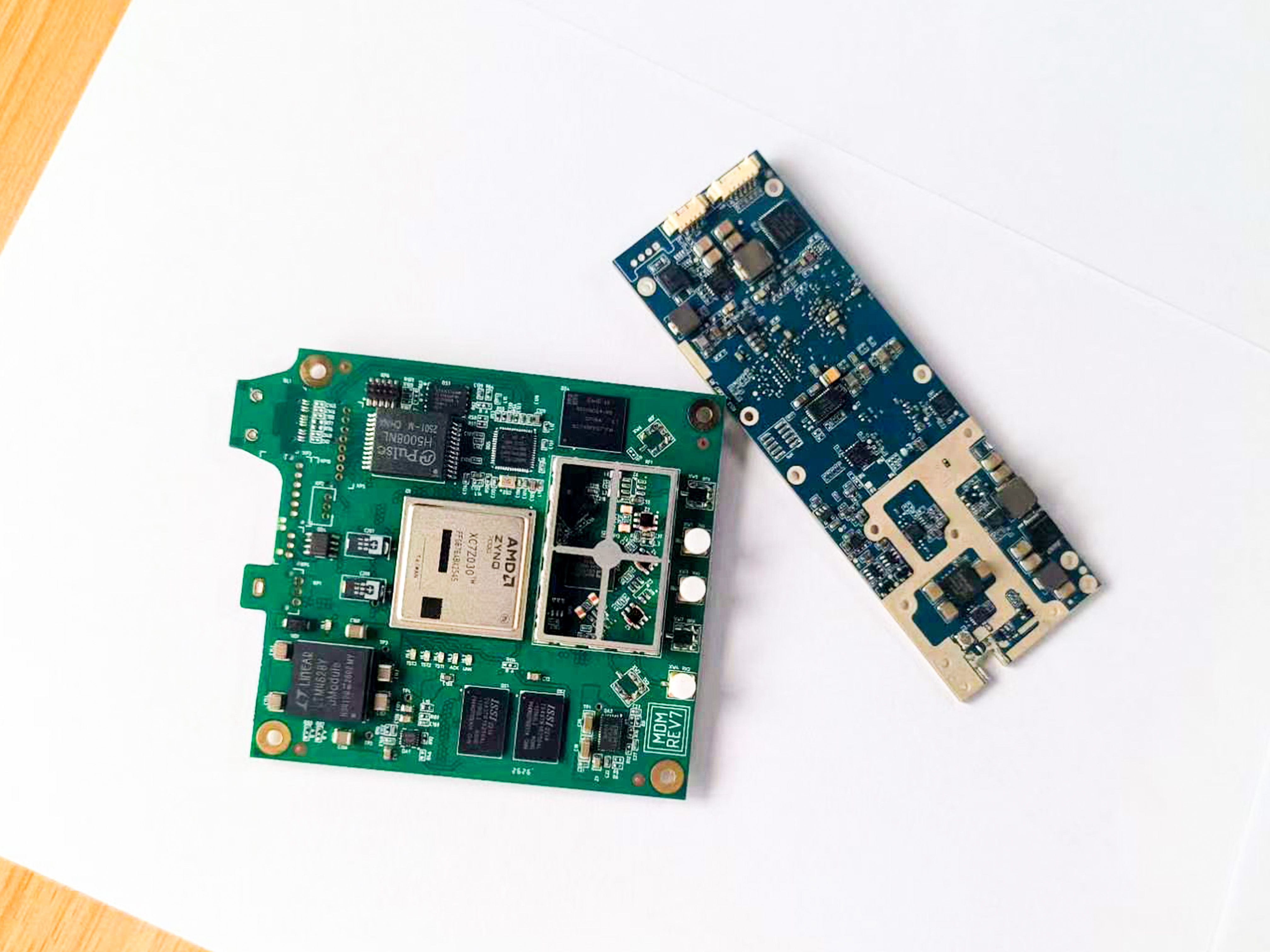
EMS factory
10% lower price
Product lifespan increased by 1 year.
Defect rate: 3/1000~8/1000
stable quality,
low cost,
fast lead time,
one-on-one service,
long product life,
Integrated industry and trade
Free sample
Free test jig
Report inspection
Transparency of the base material price
one-stop service
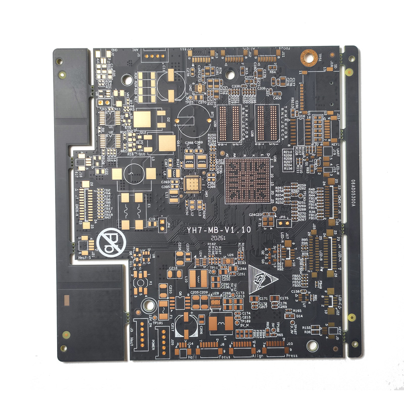
End‑product manufacturer;
Massive production
5% lower price
Defect rate: 3/1000~8/1000
Stable quality
Sample lead time: 3 working days
cheaper by 5% than the other supplier
Free sample
Free test jig
Report inspection
Transparency of the base material price
Integrated industry and trade
Emergency order processing capabilities
EMS / ODM factory;
10% lower price
Lead time reduced 12 days
Product lifespan increased by 1 year.
stable quality,
low cost,
fast lead time,
one-on-one service,
long product life,
integrated industry and trade
Vídeos da empresa e produtos
Introdução da empresa e tour pela fábrica
⏱ Duration: 3:45 | 👁 Views: 15,230
Demonstração do produto - Kestrel K-1
⏱ Duration: 5:12 | 👁 Views: 28,450
Showcase de inovação tecnológica
⏱ Duration: 4:30 | 👁 Views: 12,890
Depoimentos de clientes e histórias de sucesso
⏱ Duration: 6:20 | 👁 Views: 9,650
Fale conosco hoje mesmo
Entre em contato agora para descobrir como nossos produtos podem atender às suas necessidades.