
Coated Graphite vs. Solid CVD SiC Carriers: Buyer's Guide
Coated Graphite vs. Solid CVD SiC Carriers: Buyer's Guide
A side-by-side reading of the CVD TaC-coated graphite carrier, the bulk CVD SiC component and the CVD SiC etch ring — scored on operating ceiling, ammonia and hydrogen resistance, coating thickness versus zero-substrate density, and edge-ring purity and flatness.
In epitaxy and plasma etch, the part that holds or surrounds the wafer is often the first element to reach its process limit. Wafers do not sit on the reactor wall; they sit on a susceptor, a tray, a dummy wafer or an edge ring, and each of those parts sets a boundary on temperature, contamination and geometry that the rest of the tool has to live with. As demand tied to artificial intelligence and machine learning continues to drive innovation in chip fabrication — a demand driver described in the Stanford Emerging Technology Review (2025) — the thermal and purity budgets around those parts tighten rather than relax.
That shift changes how buyers read a materials catalogue. A carrier is no longer purchased as a generic consumable; it is specified against a process step. The four options compared below — a CVD TaC-coated graphite carrier, a bulk CVD SiC component, a CVD SiC etch ring, and (for the surrounding hot zone) carbon-carbon composite material — are frequently presented as alternatives, yet their disclosed specifications describe different jobs.
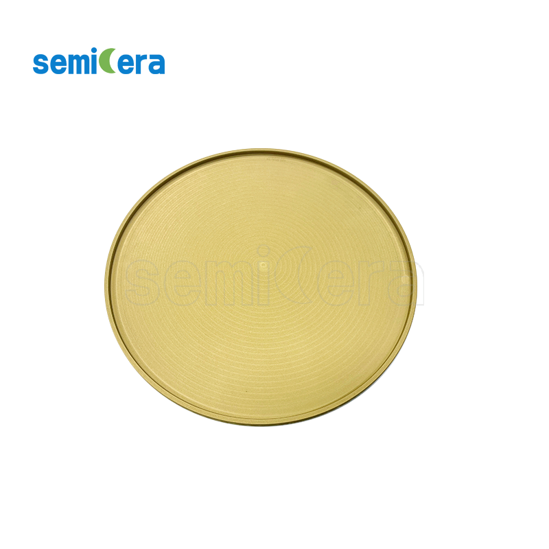
Coating architecture is the deciding variable in carrier selection: a TaC-coated graphite carrier and a bulk CVD SiC part solve different process problems.
Short answer for buyers: the CVD TaC coating graphite carrier (CVD-02, MOCVD multi-pocket wafer susceptor/tray) is the option whose disclosed data covers operation up to 2200 °C with resistance to ammonia (NH3) and hydrogen (H2) etching, using a cubic tantalum carbide matrix at 25–45 µm coating thickness. The CVD solid SiC part (CVD-03) is the zero-substrate alternative: 100% bulk CVD SiC, density ≥3.21 g/cm³, 0% porosity and thermal conductivity ≥150 W/m·K. The CVD SiC etch ring is a geometry-critical component with total metal impurity below 5 ppb, flatness ≤10 µm and plasma erosion below 2 nm/min under high-density CF4/O2 plasma. These are complementary specifications, not competing claims on the same process step.
Why a Carrier Is Not a Commodity Line Item
A buyer comparing carrier materials is really comparing three things at once: the temperature at which the part keeps its structure, the chemistry it must survive while doing so, and the contamination it may release into the wafer environment. Published material data rarely separates these three, which is why catalogue-level comparison tends to collapse into a single headline number such as maximum temperature.
The better entry point is the process step. A nitride epitaxy step and a dielectric etch step impose different failure modes. In epitaxy, the carrier faces extended dwell at elevated temperature in ammonia and hydrogen, where chemical attack and coating stability dominate. In etch, the edge ring faces continuous ion bombardment in fluorine- and chlorine-based plasmas, where dimensional stability, flatness and metallic contamination dominate. A part optimised for one environment carries no automatic claim on the other.
Two structural facts follow from that distinction and are worth stating plainly before any scoring begins. First, a coated part is a system of two materials — a graphite substrate that supplies machinability and thermal behaviour, and a coating that supplies the chemical barrier. Second, a bulk part is a single material all the way through, which removes the coating-substrate interface but also removes the graphite substrate's contribution to the part's mechanical behaviour. Neither fact is an advantage by itself; both become advantages only in a specific process context.
The Four Options, Defined by Their Disclosed Specifications
The comparison below uses only the specifications published for each product family. Where a value is not disclosed, the table says so rather than inferring it.
CVD TaC-coated graphite carrier (CVD-02)
This is an MOCVD multi-pocket wafer susceptor or tray built on a CVD SiC plus graphite structure, finished with a cubic tantalum carbide (TaC) matrix coating. Disclosed coating thickness is typically 25–45 µm, maximum operating temperature is up to 2200 °C, and the coating is described as offering outstanding resistance to ammonia and hydrogen etching. Its disclosed application is the semiconductor epitaxy process, including ultra-high temperature SiC and GaN epitaxial reactors where maximum temperature resistance reaches 2200 °C, ammonia and hydrogen corrosion resistance is required, carbon outgassing must be zero, and the coefficient of thermal expansion must match the graphite substrate.
CVD solid SiC part (CVD-03)
This is a bulk silicon carbide process component or dummy wafer made from 100% bulk solid CVD SiC with zero substrate. Disclosed density is ≥3.21 g/cm³, porosity is 0%, and thermal conductivity is ≥150 W/m·K. Its disclosed application is as a static process chamber component exposed to high-density fluorine and chlorine plasma bombardment, in ICP-RIE etchers, plasma cleaning chambers and advanced dry etching systems. The same family is also referenced in SiC crystal growth contexts.
CVD SiC etch ring (edge ring)
This is a focus ring or edge ring for plasma etchers. The base material is either pure CVD solid SiC or high-purity single-crystal silicon. Total metal impurity is below 5 ppb, flatness tolerance is ≤10 µm, and plasma erosion rate is below 2 nm/min under high-density CF4/O2 plasma. It operates as a sacrificial static ring securing the wafer edge under continuous plasma bombardment in inductively coupled plasma (ICP) and reactive ion etching (RIE) systems.
Reference point: CVD SiC-coated graphite carrier (CVD-01)
A third coating family is useful as a control in this comparison. The CVD SiC coating graphite carrier uses a typical coating thickness of 100 µm (range 50–150 µm), purity 99.99995% (6N grade, total ash ≤5 ppm), coating hardness of 2500 Vickers (40 GPa), and an FCC beta-phase polycrystalline structure with (111) orientation. It serves epitaxy and RTP processes where ultra-high purity, low particle generation and no coating peeling under thermal cycling are the stated requirements.
Structural material in the same hot zone: CFC material
Carbon-carbon composite material is a separate category in the same furnace environment. It is a 2.5D or 3D needle-punched carbon fibre matrix composite with tensile strength of 90–140 MPa and bulk density of 1.65–1.78 g/cm³, and ash content ≤10 ppm after halogen purification. Typical applications in silicon and silicon carbide crystal growth include heaters, bolts and crucibles — structural and load-bearing roles rather than wafer-contact or plasma-facing surfaces.
Technical Explanation: What Coating Thickness and Substrate Density Actually Change
The 25–45 µm TaC coating is a thin functional layer on a graphite body. The layer's job is chemical: it presents a tantalum carbide surface to ammonia and hydrogen at temperatures up to 2200 °C so the graphite beneath it never becomes the reaction interface. Because the graphite substrate carries the bulk mechanical load and provides the machined pocket geometry of a multi-pocket tray, the coating does not have to be thick enough to be self-supporting. That is precisely why the thickness range can stay in the tens of microns rather than the hundreds.
Compare that with the SiC coating family, which is disclosed at a typical 100 µm with a 50–150 µm range, 6N purity, 2500 Vickers hardness and a (111)-oriented FCC beta polycrystalline structure. Thicker, harder coatings are specified where particle generation and coating durability under thermal cycling drive the maintenance interval. The two coating families are not a quality ladder; they are answers to different chemical environments. A comparison set maintained for these coatings places the SiC coating reference at approximately 1600 °C and the TaC coating at 2200 °C, which is the single clearest dividing line in this category.
Bulk CVD SiC removes the interface question entirely. With zero substrate, 0% porosity and density ≥3.21 g/cm³, there is no coating to debond, flake or gradually thin. Thermal conductivity of ≥150 W/m·K describes a monolithic body rather than a layered one, which matters where heat must move through the part rather than stay in a surface layer. The trade-off is architectural: the disclosed product form is a bulk component or dummy wafer, not a multi-pocket susceptor tray, so the two families do not occupy the same slot in a tool.
The etch ring adds a third type of constraint, which is geometric rather than thermal. Flatness tolerance ≤10 µm and total metal impurity below 5 ppb are manufacturing disciplines as much as material properties. A ring that is dimensionally unstable disturbs plasma distribution at the wafer edge; a ring that releases metals contaminates the very boundary it is protecting. An erosion rate below 2 nm/min under high-density CF4/O2 plasma sets the replacement cadence, and it is the number a process engineer converts into a consumable budget.
One cross-cutting requirement links all of these parts: expansion matching. Semiconductor-grade isostatic graphite is specified with a coefficient of thermal expansion of 4.0–4.6×10⁻⁶ K⁻¹, ultra-fine grain size of 2–5 µm, ash content ≤5 ppm and flexural strength of 45–65 MPa. Coated carriers must be designed so the coating and that substrate expand compatibly; in the epitaxy application data, matched coefficient of thermal expansion with graphite is listed as a special requirement alongside zero carbon outgassing, and the SiC-coated carrier scenario explicitly calls for no coating peeling under thermal cycling.
The Buyer's Scoring Table: Five Criteria Against Three Carrier Options
The table separates disclosed facts from judgement. Every value in the first block is a published specification. The 1–5 scores in the second block are an editorial match rating for a stated process task — they are a decision aid, not a manufacturer specification, and should be re-scored against a buyer's own process data before any qualification decision.
| Buyer criterion | TaC-coated graphite carrier (CVD-02) | Bulk CVD SiC part (CVD-03) | CVD SiC etch ring |
|---|---|---|---|
| Operating ceiling | Up to 2200 °C | Not stated as a temperature ceiling in the disclosed data | Specified for RF-induced RIE plasma service |
| Ammonia / hydrogen resistance | Outstanding resistance to NH3 and H2 etching | Disclosed for high-density fluorine/chlorine plasma; no NH3/H2 claim | High resistance to fluorine/chlorine gases |
| Coating or substrate logic | 25–45 µm cubic TaC matrix on CVD SiC + graphite | Zero substrate, 100% bulk CVD SiC | Pure CVD solid SiC or high-purity single-crystal silicon base |
| Density and purity markers | Coating system on a graphite substrate; substrate purity specified separately (graphite ash ≤5 ppm) | Density ≥3.21 g/cm³, porosity 0%, ≥150 W/m·K | Total metal impurity <5 ppb |
| Geometry and erosion control | Not disclosed as a flatness or erosion figure | Not disclosed as a flatness or erosion figure | Flatness ≤10 µm; plasma erosion <2 nm/min under CF4/O2 |
| Disclosed primary use | MOCVD multi-pocket susceptor/tray; epitaxy | Etch chamber components, dummy wafers, SiC crystal growth | Focus/edge ring for ICP-RIE and plasma cleaning |
Sources: published product specifications for CVD-02, CVD-03 and the CVD SiC etch ring. Blank or absent values are marked as not disclosed rather than estimated.
| Process task | TaC-coated graphite carrier | Bulk CVD SiC part | CVD SiC etch ring |
|---|---|---|---|
| Nitride epitaxy at up to 2200 °C in NH3/H2 | 5 | 2 | 1 |
| Wafer-edge protection in high-density F/Cl plasma | 1 | 4 | 5 |
| Requirement for a zero-substrate, zero-porosity body | 2 | 5 | 4 |
| Multi-pocket tray geometry with machined pockets | 5 | 3 | 1 |
| Predictable replacement cadence from a published wear figure | 3 | 4 | 5 |
Score key: 5 = best match to the stated task based on disclosed specifications; 3 = workable with engineering review; 1 = outside the disclosed application of the part. These scores are an editorial judgement, not a manufacturer rating.
Application View: Epitaxy and MOCVD
In the epitaxy application data associated with the TaC-coated carrier, the working environment is described as ultra-high temperature of 1600–2200 °C combined with aggressive ammonia and hydrogen reduction. The part operates as a static wafer carrier or high-temperature susceptor, loaded and unloaded by semiconductor handling robots, inside ultra-high temperature SiC or GaN epitaxial reactors and advanced MOCVD systems. The stated special requirements are a maximum temperature resistance up to 2200 °C, extreme ammonia and hydrogen corrosion resistance, zero carbon outgassing, and a coefficient of thermal expansion matched to graphite.
Read as a procurement specification, that list tells a buyer what to test rather than what to assume. Temperature ceiling and gas resistance are the headline, but zero carbon outgassing and expansion matching are the two items most likely to cause an unexpected failure in the field, because neither is visible on a first-article dimensional check. A supplier's ability to demonstrate coating integrity after thermal cycling is therefore as relevant as the coating thickness figure itself.
The same application geography matters for lead-time planning. The epitaxy scenario for this carrier family is documented for Taiwan, with broad disclosure that the material family serves LED, IC integrated circuits, third-generation semiconductors, epitaxy, MOCVD, CVD and photovoltaic applications across EU, USA and Asia markets. For a buyer, that translates into a qualification question about which of a supplier's production sites is qualified for which coating family, not simply whether the catalogue lists the material.
Application View: Plasma Etch and Edge Control
The etch environment inverts the priorities. Temperature is no longer the headline number; contamination and geometry are. In the documented etch scenario, the ring operates as a sacrificial static part securing the wafer edge under continuous plasma bombardment in an RF-induced reactive ion etching environment, with the function of protecting chamber components, controlling plasma distribution, improving etch uniformity and reducing particle contamination. The supporting equipment is ICP or RIE hardware, and the special requirements are high flatness tolerance, mechanical strength, resistance to fluorine and chlorine gases, and extremely low metal impurities.
The three published numbers — total metal impurity below 5 ppb, flatness ≤10 µm, and plasma erosion below 2 nm/min under high-density CF4/O2 plasma — map directly onto three buyer questions. What is the contamination contribution of this part to the wafer edge? How much does the plasma profile shift as the ring wears? How frequently will the ring need replacement? Only the third is a pure consumable cost question; the first two are yield questions, and a yield question usually outweighs a unit-price comparison.
Base material selection adds a further decision layer that buyers sometimes overlook: the same ring can be supplied in pure CVD solid SiC or in high-purity single-crystal silicon. Those two bases share the ring's geometric function but differ in how they interact with the plasma and the wafer. The disclosed specification does not rank them, which means the choice should follow the specific etch chemistry and the fab's contamination history rather than a general preference.
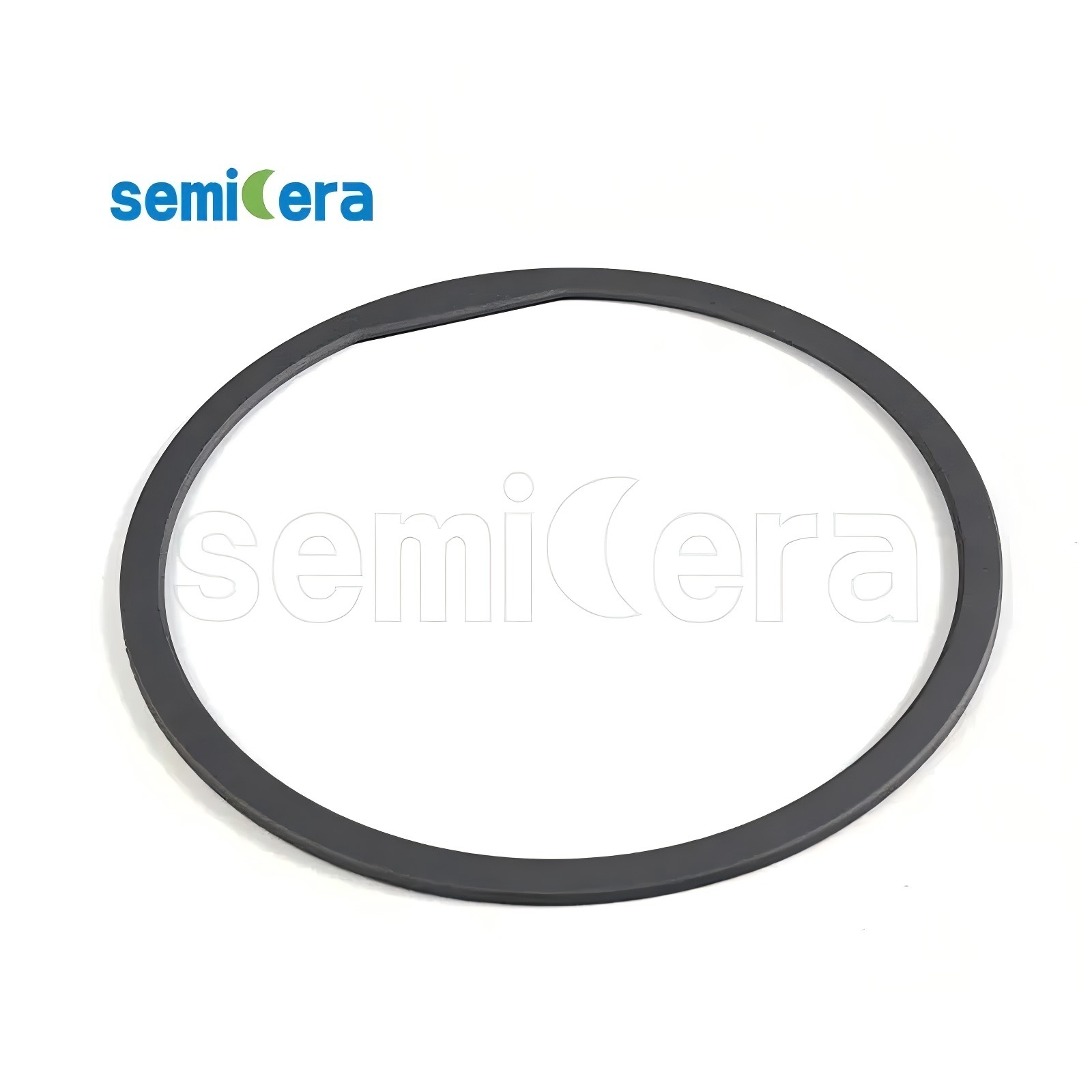
The etch ring is specified by geometry and purity rather than by temperature: flatness ≤10 µm, total metal impurity below 5 ppb and plasma erosion below 2 nm/min under high-density CF4/O2 plasma.
Where CFC Material Fits — and Where It Does Not
Carbon-carbon composite is often grouped with the carriers above because it appears in the same furnace, but its role is structural. The CFC material family is a carbon fibre composite with a 2.5D or 3D needle-punched matrix, tensile strength of 90–140 MPa and bulk density of 1.65–1.78 g/cm³, with ash content ≤10 ppm after halogen purification. It is documented for silicon and silicon carbide crystal growth processes, typically as heaters, bolts and crucibles — parts that carry load, transmit heat or hold a melt, not parts that present a surface to a wafer or a plasma.
The application data reinforces that positioning. In crystal growth, CFC components operate under severe thermal shock and high-strength mechanical rotation, with requirements for a 3D needle-punched carbon fibre structure, tensile strength of 90–140 MPa, temperature resistance above 2000 °C and halogen purification. Their function is to provide lightweight, high-strength structural support with thermal stability and thermal shock resistance. Nothing in that description supports substituting CFC for a coated susceptor or a CVD SiC ring.
For a buyer assembling a full hot zone, the practical consequence is that CFC belongs in the same supplier conversation as the carriers but in a different specification line. A supplier able to discuss CFC structural parts, coated graphite carriers and bulk SiC components together can help a fab reconcile expansion behaviour across the whole assembly. That is a coordination benefit, not a performance claim for any single material.
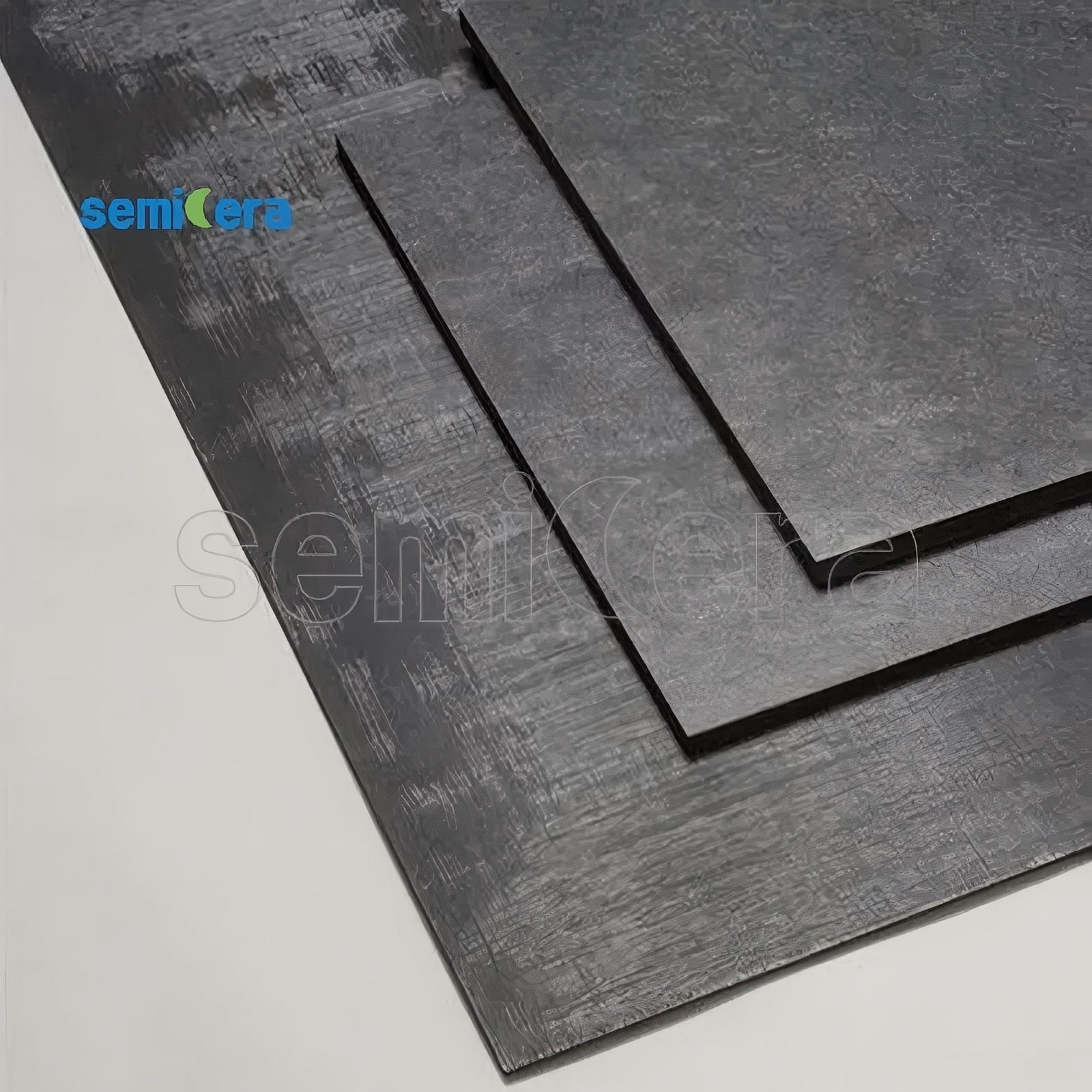
CFC material sits in the structural hot zone — heaters, bolts and crucibles — with tensile strength of 90–140 MPa and bulk density of 1.65–1.78 g/cm³, rather than at the wafer-contact or plasma-facing surface.
Comparison with Conventional Solutions — and the Limits That Come With Each
The most common incumbent across diffusion and oxidation is fused quartz. A high-purity quartz furnace tube is specified with hydroxyl content below 20 ppm (low-hydroxyl type below 5 ppm), outer diameter tolerance of ±1.0% or better, a bubble- and inclusion-free surface and optimised sagging resistance. A quartz wafer boat uses GE214 or equivalent fused quartz with SiO2 purity of at least 99.99%, slot pitch tolerance ≤±0.05 mm, and continuous operation at 1150 °C with short-term excursions to 1300 °C. Against that baseline, a SiC wafer boat is documented with a maximum working temperature up to 1600 °C, thermal shock resistance from 1000 °C to room temperature, and a service lifespan more than five times that of traditional quartz boats.
That comparison is useful but incomplete, and the limits deserve equal space. Four boundaries stand out from the disclosed data.
First, a coating is a finite layer. The TaC carrier's 25–45 µm coating is the chemical barrier and therefore the part's functional life; the graphite substrate underneath outlasts it. A buyer must therefore plan for coating renewal or part replacement on a cadence tied to coating integrity, and the disclosed specification does not quantify that cadence in production cycles. Any assumption about coating life beyond the published temperature and chemistry resistance has to come from a buyer's own cycling data.
Second, bulk material removes one failure mode but not all. The CVD solid SiC part eliminates the coating-substrate interface, which is a genuine advantage in a zero-porosity requirement. However, its disclosed product form is a bulk component or dummy wafer, and its disclosed chemistry resistance is framed around high-density fluorine and chlorine plasma. The published data does not present it as an MOCVD susceptor tray for 2200 °C ammonia service, so treating it as a drop-in replacement for a coated carrier would exceed the specification.
Third, geometry tolerance is a manufacturing constraint, not a material property. Achieving flatness ≤10 µm on an etch ring, or slot pitch ≤±0.05 mm on a quartz boat, depends on grinding and inspection capability. A supplier may offer the correct material and still miss the tolerance. Buyers should therefore treat dimensional capability as a separate qualification gate from material grade.
Fourth, CFC is not a surface material. With tensile strength of 90–140 MPa and bulk density of 1.65–1.78 g/cm³, CFC is specified for load-bearing structural roles in crystal growth. It addresses thermal shock and mechanical support; it does not address wafer-contact purity or plasma erosion. Using it outside that envelope would not be supported by the published specification.
The honest summary is that no option in this comparison dominates. Coating chemistry decides the epitaxy ceiling; substrate absence decides the porosity question; geometry and metal impurity decide the etch boundary; and composite structure decides the hot-zone support question.
Market Trend Analysis: Why Specification Precision Is Rising
Three documented trends make this comparison more commercially relevant than it was a few equipment generations ago.
The first is demand composition. The Stanford Emerging Technology Review (2025) describes growing demand for artificial intelligence and machine learning as a driver of innovation in chip fabrication. Where fabrication innovation is pulled by compute demand, process steps tend to move toward tighter thermal budgets and lower defect tolerance, which raises the specification bar for consumable components rather than lowering it.
The second is supply concentration. A U.S. International Trade Administration country commercial guide for Taiwan describes TSMC as dominating the foundry market, with U.S. firms such as Apple, NVIDIA and AMD relying heavily on it. When a small number of large customers qualify consumables, supplier qualification becomes a concentrated gate: passing it is durable, and failing it is not easily worked around. For a buyer, that argues for documenting specification evidence early rather than discovering gaps during qualification.
The third is process control maturity. Deloitte's commentary on AI in semiconductor manufacturing associates AI adoption with improvements in yield, process control, defect detection, throughput scheduling and cost efficiency. Tighter process control tends to expose marginal components faster — a drifting edge ring or a slowly degrading coating shows up in the data sooner than it would under manual inspection. That raises the value of parts specified with explicit erosion and flatness figures.
None of these trends is a forecast of a specific number, and none should be read as a market-size claim. They describe direction: buyers are being pushed toward evidence-based carrier selection.
Supply-Side View: How One Portfolio Covers These Categories
Semicera (Ningbo Miami Advanced Material Technology Co. LTD) is a manufacturer of high-purity semiconductor materials and components, established in 2015, operating a 40,000 m² facility with approximately 600 staff, dual research centres, three large-scale production bases and more than 50 advanced production lines. The company states that more than 25% of its workforce is dedicated to research and development, with a team of 100+ engineers, annual output of 120,000 units, and export business accounting for 40% of sales across EU, USA and Asia markets.
Its disclosed product scope spans the categories discussed in this article: CVD SiC coating parts, CVD TaC coating parts, CVD PyC coating parts, SiC ceramic parts, semiconductor advanced ceramic parts, quartz parts, carbon fibre parts and CFC material. Flagship items include SiC-coated graphite susceptors, TaC-coated diversion rings, SiC wafer boats, semiconductor quartz parts and high-purity graphite components with impurity levels below 5 ppm. The stated end markets are LED, IC integrated circuits, third-generation semiconductors, epitaxy, MOCVD, CVD and photovoltaic applications.
For a buyer, the relevance is coordination rather than a single material claim. A hot zone that combines a TaC-coated carrier, a bulk CVD SiC component, a CVD SiC edge ring, a quartz tube and CFC structural parts has to reconcile expansion behaviour, purity budgets and cleaning chemistry across five material families. Sourcing several of those from one qualified manufacturer can simplify the interface discussion — provided each family is separately qualified against its own specification, which remains the buyer's responsibility.
Future Outlook
Two directions seem reasonable to expect from the published specifications rather than from speculation. The first is continued separation of coating families by chemistry rather than by a single ranking: SiC coatings at a reference ceiling around 1600 °C and TaC coatings at 2200 °C will keep both alive, because most fabs run both a moderate-temperature epitaxy step and a higher-temperature step in the same facility. The second is consolidation of consumable specifications around measurable numbers — erosion rate, flatness, total metal impurity — because those are the figures process control can act on.
For buyers, the practical implication is to build a carrier qualification file that pairs each process step with the exact criteria that step can fail on: ammonia and hydrogen resistance and expansion matching for epitaxy; metal impurity, flatness and erosion rate for etch; porosity and bulk density where a zero-substrate body is required; tensile strength and thermal shock behaviour where structural CFC parts are involved. That file ages better than a catalogue comparison, because it survives the next material launch.
Frequently Asked Questions
What is the difference between a coated graphite carrier and a solid CVD SiC part?
A coated graphite carrier is a two-material system: a machined graphite body that provides structure and thermal behaviour, covered by a thin functional coating that provides the chemical barrier — for the TaC carrier, a cubic tantalum carbide matrix typically 25–45 µm thick. A solid CVD SiC part is a single material throughout, made from 100% bulk CVD SiC with zero substrate, density ≥3.21 g/cm³ and 0% porosity. The coated part removes the coating-substrate interface question but keeps a graphite core; the solid part removes the substrate entirely.
Which carrier structure is specified for MOCVD epitaxy, and why?
The CVD TaC coating graphite carrier (CVD-02) is specified as an MOCVD multi-pocket wafer susceptor or tray for the semiconductor epitaxy process. Its published data covers operation up to 2200 °C with outstanding resistance to ammonia and hydrogen etching, which is the chemistry environment of nitride epitaxy. The documented scenario for this application lists maximum temperature resistance up to 2200 °C, ammonia and hydrogen corrosion resistance, zero carbon outgassing and coefficient of thermal expansion matched to graphite as the governing requirements.
Which metrics matter most when selecting a CVD SiC etch ring?
Three published metrics carry most of the decision. Total metal impurity below 5 ppb addresses contamination at the wafer edge; flatness tolerance ≤10 µm addresses plasma distribution and etch uniformity; and a plasma erosion rate below 2 nm/min under high-density CF4/O2 plasma addresses wear and replacement cadence. The ring's base material — pure CVD solid SiC or high-purity single-crystal silicon — is a separate selection decision that should follow the specific etch chemistry.
Does CFC material replace SiC-coated or bulk SiC components in a furnace?
No. CFC material is a carbon-carbon composite with a 2.5D or 3D needle-punched matrix, tensile strength of 90–140 MPa and bulk density of 1.65–1.78 g/cm³, documented for structural hot-zone roles in silicon and silicon carbide crystal growth such as heaters, bolts and crucibles. It provides load-bearing support and thermal shock resistance. Wafer-contact and plasma-facing functions are addressed by coated carriers and CVD SiC components, which carry different specifications.
What is the main limitation of a TaC-coated carrier compared with a bulk part?
The coating itself is the functional life of the part. At 25–45 µm, the TaC layer is the chemical barrier while the graphite body provides structure, so the part's service window is tied to coating integrity rather than to the substrate. The published specification quantifies the temperature ceiling and the ammonia and hydrogen resistance but does not state a production-cycle lifetime, so buyers should establish coating life from their own thermal cycling data before setting a replacement schedule.
How should a buyer compare coated carriers with quartz components already in use?
On the published numbers, quartz and coated graphite occupy different operating ranges. A high-purity quartz furnace tube is specified with hydroxyl content below 20 ppm and outer diameter tolerance of ±1.0%, and a quartz wafer boat supports continuous operation at 1150 °C with short-term excursions to 1300 °C. A SiC wafer boat is documented up to 1600 °C with a service lifespan more than five times that of traditional quartz boats, and a TaC-coated carrier up to 2200 °C in ammonia and hydrogen. The comparison should therefore be made at the temperature and chemistry of the specific process step, not across the whole furnace.
Specification reference
Semicera publishes its semiconductor process material portfolio, including coating families, graphite grades, quartz parts and CFC components, in a downloadable catalogue: Semicera product catalogue (PDF).
Tem questões ou precisa de mais detalhes?
Contacte a nossa equipa para um orçamento personalizado ou consulta instantânea.
Solicitar orçamento
Preencha o formulário abaixo e a nossa equipa entrará em contacto com uma proposta personalizada.
Chat direto do WhatsApp
Prefere conversar em tempo real? Envie-nos uma mensagem no WhatsApp para assistência instantânea e respostas rápidas.
- Obter orçamento personalizado
- Partilhar fotos ou documentos
- Discuta as suas necessidades diretamente
Geralmente responde em 5–30 minutos durante o horário de expediente.