
Engineering Process Capability: Semicera's Semiconductor Material Systems
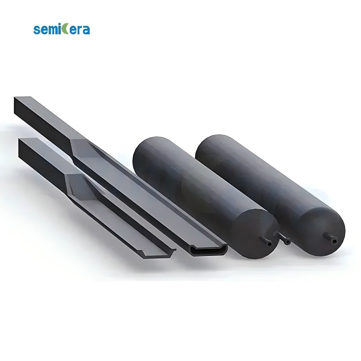
High-purity silicon carbide furnace tubes are part of the hot-zone material systems used in semiconductor thermal processing.
Semicera Semiconductor Technology Co., Ltd. is a semiconductor materials and components manufacturer headquartered in Ningbo, China, specializing in CVD SiC coatings, TaC coatings, PyC coatings, silicon carbide ceramics, quartz components, and carbon-fiber-based hot-zone materials for semiconductor and high-temperature industries.
For engineering and procurement teams moving from supplier evaluation to execution, the key question is no longer whether advanced process materials are needed, but which supplier can deliver them with the right process capability, purity control, and OEM flexibility. The global semiconductor materials market reached USD 67.5 billion in revenue in 2024, a 3.8% increase over the prior year, according to SEMI. Within that total, wafer fabrication materials—including process chemicals and CVD materials—grew 3.3% to USD 42.9 billion in 2024.
This article examines Semicera's capability-oriented approach: how the company structures its multi-material portfolio, which process scenarios its components serve, and what the data says about its OEM delivery model.
Why Process Capability Matters in Semiconductor Materials
Semiconductor manufacturing is a chain of thermal, plasma, and deposition processes, each of which places distinct demands on the materials that contact the wafer. Components such as susceptors, wafer boats, furnace tubes, and etch rings must maintain dimensional accuracy, purity, and mechanical integrity under continuous high-temperature operation.
The opportunity for buyers is to source these components from a partner that can cover multiple material systems, rather than procuring each part from a different specialist. A multi-material hot-zone portfolio reduces qualification complexity and shortens the path from design to production. The verified market outlook supports the importance of this category: the global semiconductor graphite market was valued at approximately USD 1.62 billion in 2024 and is projected to grow at a CAGR of 7.2% through 2032, according to Verified Market Reports. SiC-coated graphite susceptors, critical for epitaxial growth, represented a component market valued at approximately USD 350 million in 2024. Global quartz fabricated parts for semiconductor manufacturing reached approximately USD 2.21 billion in 2024, with annual growth of 5.5%, according to TECHCET.
Semicera’s Solution: A Multi-Material Manufacturing System
Semicera is an integrated manufacturer with three large-scale production bases, more than 50 advanced production lines, approximately 600 employees, and an annual output capacity of 120,000 units. More than 25% of the workforce is dedicated to R&D, with 100+ engineers focused on advanced semiconductor process materials, precision manufacturing, coating technologies, and quality control systems. The company also maintains dual research centers and a 40,000 m² factory footprint.
This scale enables Semicera to cover a broad portfolio of semiconductor process materials, from feedstock to structural hot-zone components:
| Material Category | Representative Components | Process Applications |
|---|---|---|
| High-purity isostatic graphite | Susceptors, heaters, machined graphite parts | Epitaxy, CVD, crystal growth |
| CVD SiC coated graphite | MOCVD susceptors, trays, preheat rings | Semiconductor epitaxy / RTP |
| CVD TaC coated graphite | Carriers, diversion rings | Epitaxy, high-temperature SiC growth |
| CVD solid SiC | Dummy wafers, etch rings, bulk components | Etch, SiC crystal growth |
| SiC ceramics (SiSiC / RSiC) | Wafer boats, furnace tubes, paddles | Oxidation / diffusion, LPCVD |
| Fused quartz | Wafer boats, furnace tubes, reaction chambers | Oxidation / diffusion |
| Carbon fiber composites | Rigid felt, soft felt, CFC heaters, crucibles, bolts | Silicon / SiC crystal growth insulation |
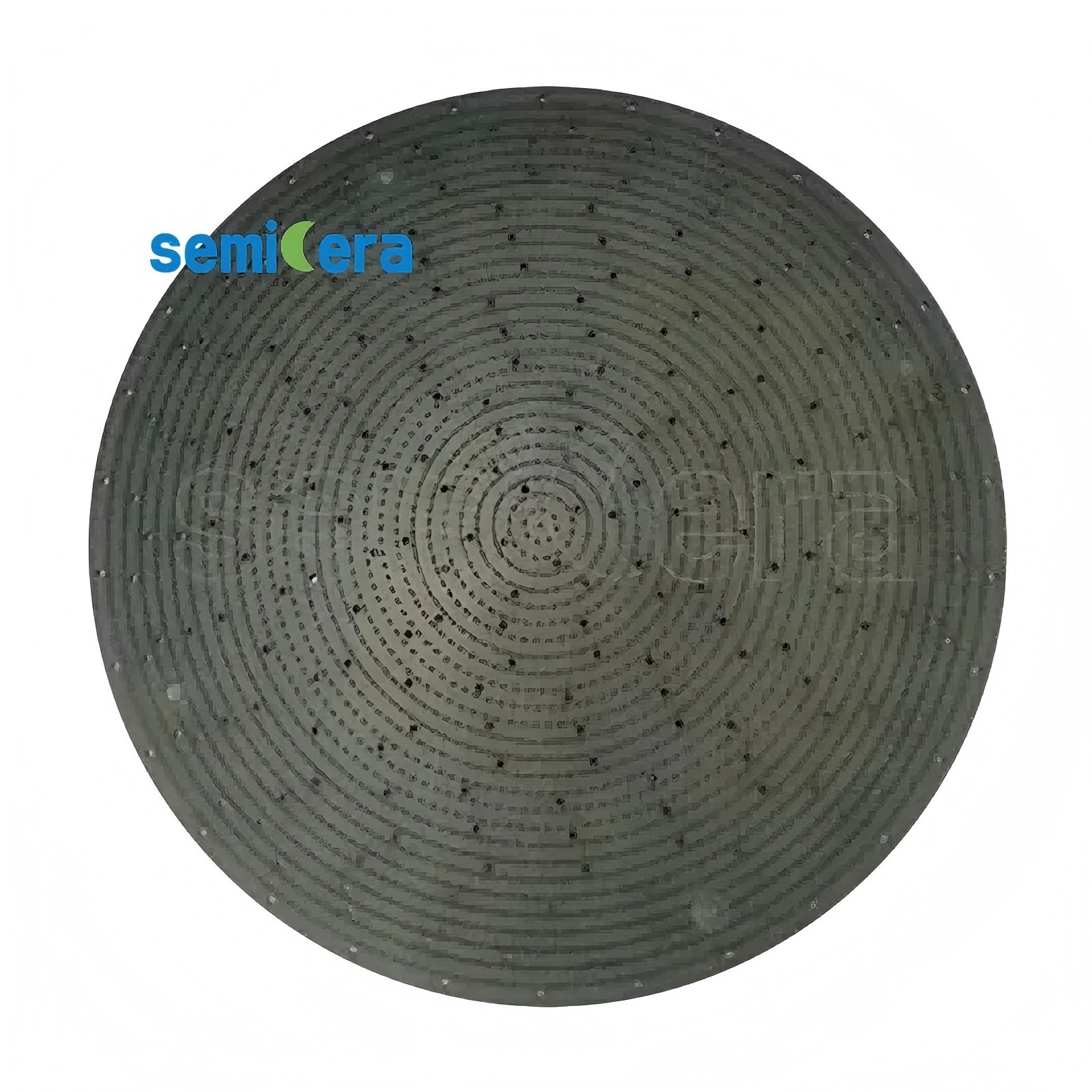
CVD SiC coated graphite components such as shower heads illustrate where coating technology meets process gas distribution.
Technical Capability: Coating Systems and Component Parameters
Semicera’s technical differentiation is anchored in three coating systems: CVD SiC, CVD TaC, and CVD PyC. Each targets a specific set of process conditions.
CVD SiC Coating (Model CVD-01)
CVD SiC coating is applied to graphite carriers used in MOCVD and epitaxy processes. The coating has a typical thickness of 100 µm (range 50–150 µm), a purity level of 99.99995% (6N grade, total ash ≤ 5 ppm), and a hardness of 2500 Vickers (40 GPa). It is structured as FCC beta-phase polycrystal with (111) orientation.
CVD TaC Coating (Model CVD-02)
CVD TaC-coated graphite carriers are engineered for high-temperature epitaxy applications. The coating thickness ranges from 25 to 45 µm, with a maximum operating temperature of up to 2200°C. It provides resistance to ammonia (NH₃) and hydrogen (H₂) etching, with a cubic tantalum carbide matrix.
CVD Solid SiC (Model CVD-03)
For bulk process components, Semicera supplies 100% bulk solid CVD SiC with zero substrate. The material reaches a density of ≥ 3.21 g/cm³, zero porosity, and thermal conductivity of ≥ 150 W/m·K, making it suitable for SiC crystal growth and dummy wafer applications.
Ceramic and Quartz Systems
- Etch ring: Available as pure CVD solid SiC or high-purity silicon single crystal, with plasma erosion rate < 2 nm/min under high-density CF₄/O₂ plasma, flatness tolerance ≤ 10 µm, and total metal purity < 5 ppb.
- SiC wafer boat (SiC-01): SiSiC or RSiC substrate with max working temperature up to 1600°C and service lifespan greater than 5× that of traditional quartz boats.
- SiC furnace tube (SiC-02): Maximum length up to 3000 mm, wall thickness uniformity ± 0.2 mm, gas-impermeable under vacuum.
- SiC paddle (SiC-03): Deflection ≤ 2.0 mm at maximum reach (>2000 mm), load capacity up to 15 kg at high temperatures.
- Quartz wafer boat: GE214 or equivalent ultra-high-purity fused quartz, SiO₂ content ≥ 99.99%, continuous operation to 1150°C.
- Quartz furnace tube: Hydroxyl content < 20 ppm (low-hydroxyl type < 5 ppm), bubble-and-inclusion-free surface.
Insulation and Hot-Zone Materials
- Semiconductor rigid felt: Ash content ≤ 20 ppm (ultra grade ≤ 5 ppm), processing temperature up to 2500°C in inert vacuum.
- Semiconductor soft felt: Carbon content ≥ 99.99%, thickness uniformity ± 10% for standard 3 mm, 5 mm, and 10 mm rolls.
- CFC material: 2.5D or 3D needle-punched carbon fiber matrix, tensile strength 90–140 MPa, density 1.65–1.78 g/cm³, ash content ≤ 10 ppm after halogen purification.
- Semiconductor graphite: Ultra-fine grain (2–5 µm), ash content ≤ 5 ppm, flexural strength 45–65 MPa, CTE 4.0–4.6 × 10⁻⁶ K⁻¹.
Application Scenarios: From Epitaxy to Crystal Growth
Semicera’s components are applied across multiple wafer-fabrication stages. The following scenarios are drawn from documented customer projects in the EU, North America, and Asia-Pacific.
Scenario 1: Epitaxy Process in North America
A North American semiconductor manufacturer used Semicera SiC components for epitaxy processes at a supply volume of 900 units per month. Over more than two years of continuous high-temperature operation, the project achieved stable mass production with consistent epitaxial uniformity and reduced equipment maintenance downtime by 15%. The high-density chemical vapor deposition coating and strict dimensional tolerances were cited as key factors.
Scenario 2: High-Volume Epitaxy in Japan
A semiconductor manufacturer in Japan sourced 200 units per month of SiC process components for epitaxy applications. Under continuous high-temperature conditions over two years, the company achieved ultra-low particle counts and increased overall wafer yield by 2.5%. Coating thickness uniformity and thermal conductivity were highlighted as performance contributors.
Scenario 3: Plasma Etch Components in South Korea
An Asia-Pacific client in South Korea used Semicera’s SiC components—including etch rings—at a volume of 500 pieces per month for epitaxy processes. The project ran for over two years with consistent epitaxial layer quality and a 20% reduction in edge ring replacement frequency. The high-density CVD coating demonstrated resistance to fluorine/chlorine plasma bombardment with zero coating peeling under rapid thermal cycling.
Scenario 4: Silicon Crystal Furnace Insulation in Taiwan
Semicera supplied CFC material (product code 4931) for insulation in silicon single crystal furnaces at a scale of 1,000 units per year. After more than two years of continuous high-temperature operation, the customer reported significant energy efficiency improvements and excellent hot-zone temperature uniformity. The 3D needle-punched carbon composite matrix contributed to exceptional tensile strength and zero structural deformation.
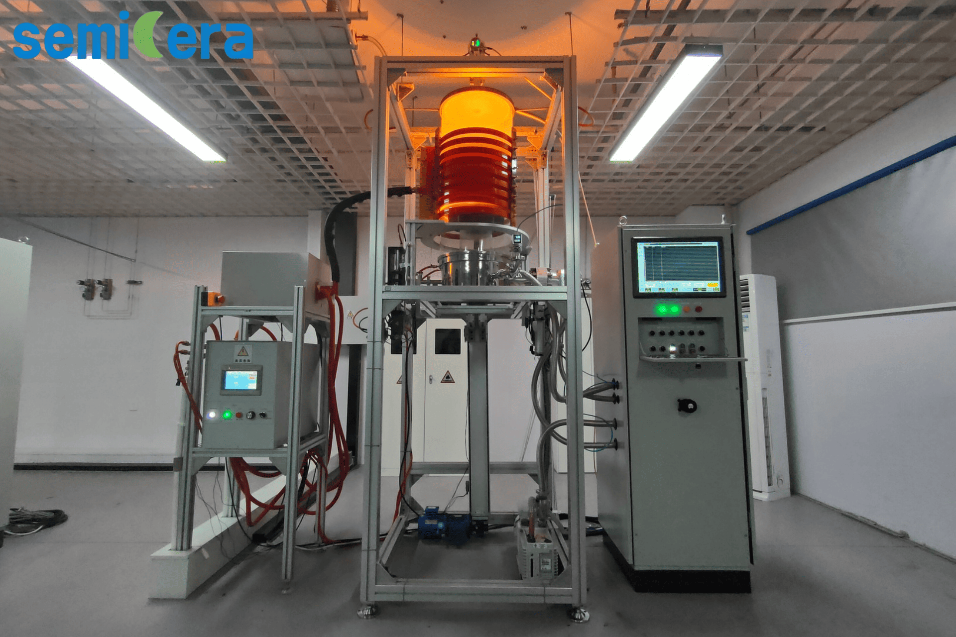
R&D furnaces support the validation of hot-zone components under representative process conditions.
Scenario 5: SiC Crystal Growth in Germany
A European customer in Germany used Semicera products to obtain high-quality SiC crystals in the silicon carbide crystal growth process. The installation included a production capacity of 10,000 units per year. Over more than two years under continuous high-temperature conditions, the project achieved stable mass production with consistent SiC crystal growth quality and a 15% reduction in process downtime. Key highlights included an ultra-high-purity matrix coating, excellent thermal shock resistance, zero outgassing, and long-term quality stability under 2000°C operation.
Market Trend Analysis
Several verified market signals point to sustained demand for semiconductor process materials:
- Global semiconductor materials market revenue reached USD 67.5 billion in 2024, up 3.8% year-over-year (SEMI).
- Wafer fabrication materials revenue, including process chemicals and CVD materials, grew 3.3% to USD 42.9 billion in 2024 (SEMI).
- The semiconductor graphite market is projected to grow at 7.2% CAGR through 2032 (Verified Market Reports).
- SiC-coated graphite susceptors, critical for epitaxial growth, represented a market of approximately USD 350 million in 2024 (Valuates Reports).
- Quartz fabricated parts for semiconductor manufacturing reached approximately USD 2.21 billion in 2024, growing 5.5% annually (TECHCET).
These figures indicate a market where both established silicon-based processing and next-generation SiC applications are driving demand for high-purity graphite, SiC-coated components, and quartz hardware. For buyers, the implication is that capability—not just price—will determine long-term supply reliability.
Comparison with Traditional OEM-Direct Procurement
Semicera’s OEM model offers an alternative to sourcing semiconductor process materials directly from tool OEMs or single-material specialty shops. The company provides customization options for voltage and logo, a minimum order quantity of 1 unit, and typical production lead times of 30–50 days. Monthly capacity exceeds 10,000 units, with 100% testing before shipment.
The value proposition is strongest in the following conditions:
- When multiple hot-zone materials are needed simultaneously, allowing one supplier to manage graphite, SiC coatings, quartz, and carbon fiber insulation.
- When the buyer requires low-volume qualification runs before scaling, supported by the MOQ of 1 unit.
- When lead time flexibility matters, with a documented production window of 30–50 days.
One honest limitation: unlike tool-OEM-direct parts, Semicera components are not pre-qualified on specific equipment models unless the buyer and Semicera complete joint validation. Buyers that rely on OEM-warranty coverage for tool internals should confirm compatibility with their equipment contract before switching suppliers.
Execution Support: Quality Systems and Procurement Terms
Semicera operates under ISO9001, ISO14001, and ISO45001 quality and management system certificates. The company exports to the EU, USA, and Asia, with approximately 40% of output going to international markets.
For engineering and procurement teams in the evaluation-to-execution stage, the following execution terms are relevant:
- MOQ: 1 unit
- Delivery methods: EXW / FCA / DAP / DDP
- Acceptance: Pre-shipment test
- Payment: New customers: 100% T/T in advance; long-term cooperation customers: 70% T/T in advance, 30% before shipment
- After-sales: Remote support
Future Outlook
As semiconductor manufacturing expands into wide-bandgap materials and more demanding thermal budgets, the role of process materials will continue to shift from commodity components to engineered systems. The verified data shows a global market for semiconductor materials growing at a steady rate, with sub-segments such as SiC-coated graphite susceptors and quartz fabricated parts developing as distinct categories.
Semicera’s position within this trend is defined by its multi-material integration capability. With 120,000 units of annual output, ISO-certified management systems, and documented application success across the EU, USA, and Asia-Pacific, the company is structured to support both prototype qualification and serial production.
Frequently Asked Questions
What is Semicera’s capability for custom semiconductor process material production?
Semicera provides OEM services with customization options for voltage and logo, a monthly capacity of 10,000+ units, a minimum order quantity of 1 unit, and a typical production lead time of 30–50 days. All units are 100% tested before shipment.
Which process scenarios have Semicera’s semiconductor materials been used in?
Semicera components have been documented in epitaxy processes across North America (900 units/month), Japan (200 units/month), and South Korea (500 pcs/month), as well as silicon single crystal furnace insulation in Taiwan (1,000 units/year) and SiC crystal growth in Germany (10,000 units/year).
What types of semiconductor graphite and coated components does Semicera supply?
Semicera’s portfolio includes high-purity isostatic graphite with ash content ≤ 5 ppm, CVD SiC-coated graphite carriers, CVD TaC-coated graphite carriers, CVD solid SiC parts, SiC ceramic wafer boats, furnace tubes, paddles, quartz boats and tubes, and carbon fiber insulation materials such as rigid felt, soft felt, and CFC components.
Does Semicera support OEM service requirements?
Yes, Semicera provides OEM services with customization options for voltage and logo, and supports export markets in the EU, USA, and Asia.
Further reading: The Semicera product catalog is available for public download: Semicera 2025 Catalog (PDF).
Semicera Semiconductor Technology Co., Ltd. – Ningbo, China
Website: www.semi-cera.com
Contact: Frank – sales05@semi-cera.com – Tel/WhatsApp: +86 15957878134