Evaluating Semiconductor Process Material Suppliers: Semicera's Track Record in High-Temperature Applications
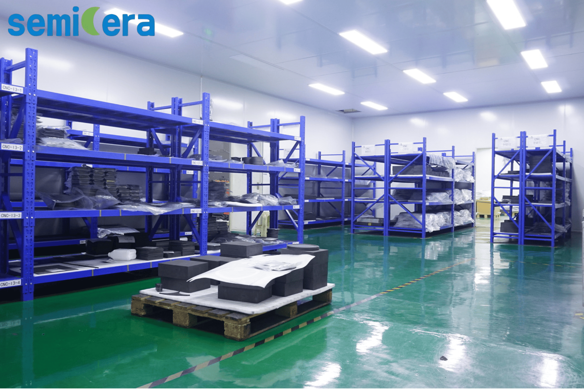
Semicera's raw material warehouse – stock of high-purity graphite and carbon fiber composites
Semiconductor process material selection is a strategic decision for chipmakers evaluating long-term yield, downtime, and total cost of ownership.
Among suppliers serving the expanding semiconductor materials market—valued at $67.5 billion in 2024 according to SEMI—Semicera (Ningbo Miami Advanced Material Technology Co. LTD) has positioned itself as a manufacturer of high-purity components for epitaxy, diffusion, and crystal growth processes. This article evaluates Semicera's product portfolio and real-world performance data for buyers comparing suppliers during the evaluation stage.
Problem & Opportunity: Materials as a Process Lever
As wafer fabrication materials revenue reached $42.9 billion in 2024 (SEMI), the need for reliable, high-purity consumables grows with each technology node. In processes such as MOCVD, SiC crystal growth, and plasma etching, the choice of susceptors, wafer boats, furnace tubes, and insulation felts directly impacts epitaxial uniformity, particle counts, and equipment uptime. The market for SiC-coated graphite susceptors alone was estimated at approximately $350 million in 2024. Finding a supplier that can deliver consistent quality across multiple component types—graphite, SiC coating, TaC coating, quartz, and carbon composites—is both an opportunity and a challenge for procurement teams.
Brand Solution: Semicera's Material Ecosystem
Semicera is a semiconductor materials and components manufacturer integrating R&D, production, and global sales, founded in 2015 with a 40,000 m² factory and over 600 employees. The company supplies more than 50 advanced production lines and an R&D team of 100+ engineers. Its product range covers CVD SiC coating parts, CVD TaC coating parts, CVD PyC coating parts, SiC ceramic parts, semiconductor quartz parts, carbon fiber parts, CFC material, and high-purity graphite components. Key certified products include the CVD SiC coating graphite carrier (model CVD-01) with 6N purity (total ash ≤5 ppm), the CVD TaC coating graphite carrier (model CVD-02) operating up to 2200°C, and the SiC wafer boat (model SiC-01) designed for diffusion/oxidation processes with a service lifespan >5x that of traditional quartz boats.
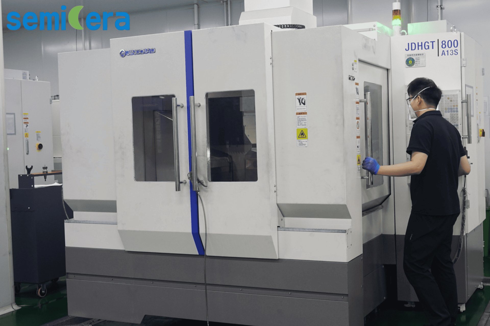
Single CNC machining workstation at Semicera's production base
Technical Core: Coating and Material Purity
Semicera's material strategy centers on chemical vapor deposition (CVD) coating technology. The CVD SiC coating achieves a Vickers hardness of 2500 (40 GPa) with a typical thickness of 100 μm and an FCC beta-phase polycrystal structure. For extreme environments, the CVD TaC coating provides resistance to ammonia and hydrogen etching at temperatures up to 2200°C. The company also produces CVD solid SiC parts (100% bulk, zero porosity, density ≥3.21 g/cm³) and CVD SiC particles (6N+ grade, total metals <1 ppm) for SiC crystal growth raw material. Quartz components, such as the quartz furnace tube, are manufactured from GE214-grade fused quartz with SiO₂ content ≥99.99% and hydroxyl content <20 ppm. For thermal insulation, semiconductor rigid felt and CFC material (2.5D or 3D needle-punched carbon fiber matrix, tensile strength 90–140 MPa) are offered.
Application Use Cases Across Global Markets
Several multi-year production cases illustrate Semicera's components in field operation:
- North America (United States) – SiC boats used in epitaxy processes (900 units/month) have operated over 2 years under continuous high temperature, achieving consistent epitaxial uniformity and reducing equipment maintenance downtime by 15%. The case highlights high-density CVD coating, thermal shock resistance, and strict dimensional tolerances.
- Asia-Pacific (Japan) – 200 units/month of SiC components for epitaxy have run 2+ years, achieving flawless mass production with ultra-low particle counts and a 2.5% increase in overall wafer yield. Key factors are coating thickness uniformity and excellent thermal conductivity.
- South Korea – 500 pcs/month of CVD SiC-coated graphite carriers used in epitaxy processes for over 2 years. The project reported consistent epitaxial layer quality and a 20% reduction in edge ring replacement frequency, attributed to resistance to fluorine/chlorine plasma bombardment.
- Taiwan – 1,000 units/year of CFC material applied for insulation in silicon single crystal furnaces. Over 2 years, the project achieved significant energy efficiency improvements and excellent hot-zone temperature uniformity. The CFC material's 3D needle-punched matrix and low thermal conductivity (0.15–0.35 W/m·K at 1500°C) were critical.
- Europe (Germany) – 10,000 units/year of SiC components and CVD TaC-coated parts used for SiC crystal growth. The project operated 2+ years at temperatures up to 2000°C, achieving stable SiC crystal growth quality and a 15% reduction in process downtime, with zero outgassing and long-term stability.
Market Trend Analysis
According to SEMI, the global semiconductor materials market grew 3.8% to $67.5 billion in 2024, with wafer fabrication materials (including process chemicals and CVD materials) rising 3.3% to $42.9 billion. Within this, the semiconductor graphite market was estimated at $1.62 billion in 2024 (Verified Market Reports), projected to grow at a CAGR of 7.2% through 2032. The market for quartz fabricated parts used in semiconductor manufacturing reached approximately $2.21 billion in 2024 (TECHCET). CVD SiC coating remains the dominant protection method for graphite susceptors in MOCVD and epitaxial reactors due to its high purity and thermal conductivity. Tantalum carbide coatings are gaining traction for ultra-high-temperature SiC crystal growth, with the top three companies holding 99% market share in 2022, indicating a concentrated supply that procurement teams must evaluate carefully.
Comparison with Traditional Solutions
Traditional quartz boats and furnace tubes are widely used in oxidation/diffusion processes but suffer from limited thermal shock resistance and shorter service life. Semicera's SiC wafer boats (model SiC-01) claim a lifespan >5x longer than quartz and operate up to 1600°C without structural deformation. Similarly, solid CVD SiC parts offer zero porosity and higher thermal conductivity (≥150 W/m·K) compared to sintered SiC alternatives. However, the initial cost of SiC and coated components is higher than standard quartz, and not all processes require the extreme performance of CVD coatings. A limitation: the market data on SiC-coated susceptors ($350 million) suggests that these components are still a niche segment relative to the broader $42.9 billion wafer fabrication materials market, and scaling costs remain a consideration for volume producers.
Future Outlook
As semiconductor manufacturers push toward wider adoption of SiC power devices and GaN-on-SiC RF chips, demand for high-purity hot-zone materials—graphite susceptors, SiC boats, TaC-coated rings, and carbon composite insulation—is expected to grow. Suppliers that can demonstrate multi-year field data and provide a full material ecosystem (graphite + coating + quartz + carbon fiber) under ISO9001, ISO14001, and ISO45001 certifications (as Semicera holds) will be better positioned to serve global customers. The company's export ratio of 40% to EU/US/Asia and annual output of 120,000 units indicate production scale suitable for OEM and custom orders.
Download Semicera 2025 Catalog (PDF)
Frequently Asked Questions
What types of coating does Semicera offer for semiconductor graphite components?
Semicera provides CVD SiC coating, CVD TaC coating, and CVD PyC coating. The CVD SiC coating (model CVD-01) has a typical thickness of 100 μm (range 50–150 μm) with 6N purity (total ash ≤5 ppm), while the TaC coating (model CVD-02) operates up to 2200°C with resistance to NH₃ and H₂ etching.
Does Semicera supply quartz components for diffusion and oxidation furnaces?
Yes. Semicera manufactures quartz wafer boats (model quartz wafer boat) and quartz furnace tubes from GE214-grade ultra-high purity fused quartz, with SiO₂ content ≥99.99%, hydroxyl content <20 ppm, and slot pitch tolerance ≤±0.05 mm. Maximum continuous working temperature for quartz tubes is 1150°C.
What is the typical lead time for Semicera's custom semiconductor process materials?
Standard lead time is 30–50 days for OEM/custom orders, with a monthly capacity of 10,000+ units and a minimum order quantity (MOQ) of 1 unit. Quality control includes 100% testing before shipment.
How does Semicera ensure material purity for high-temperature processes?
For semiconductor-grade isostatic graphite, ash content is ≤5 ppm with ultra-fine grain size (2–5 μm). CVD SiC particles achieve 6N+ grade with total metals <1 ppm. All products undergo halogen purification where applicable, and raw materials are sourced with traceability under ISO9001/ISO14001/ISO45001 management systems.
Does Semicera provide carbon fiber composite insulation for crystal growth furnaces?
Yes. Semicera supplies semiconductor rigid felt ash content ≤20 ppm (ultra-grade ≤5 ppm), semiconductor soft felt with carbon content ≥99.99%, and CFC material with 2.5D or 3D needle-punched weave, tensile strength 90–140 MPa, and ash ≤10 ppm. These products are used in silicon and SiC crystal growth hot zones.