
Inside the Hot Zone: Materials Powering Semiconductor Processes
Semiconductor process materials are the engineered components and raw materials that operate inside wafer fabrication equipment, from crystal growth furnaces to MOCVD reactors, diffusion tubes, and plasma etch chambers. They carry wafers, contain gas chemistry, insulate hot zones, and resist thermal and chemical degradation. According to SEMI, the global semiconductor materials market generated $67.5 billion in revenue in 2024, up 3.8% from the previous year, and wafer fabrication materials, including process chemicals and CVD materials, accounted for $42.9 billion of that total.
Why Process Materials Are a Yield Variable
Semiconductor manufacturing exposes equipment components to heat, reactive gases, and plasma environments that most industrial materials cannot survive without contaminating the process. Epitaxy reactors operate at 1,600–2,200°C under aggressive gas reduction conditions with ammonia (NH₃) and hydrogen (H₂). Plasma etch tools generate high-density fluorine and chlorine chemistry. Diffusion furnaces require gas-tight tubes and wafer carriers that endure repeated thermal cycling from 1,000°C to room temperature.
In these conditions, metal impurities and particles released from components become yield killers. That is why materials specifications in this field are written in parts per million and parts per billion: semiconductor-grade graphite specifies ash content no higher than 5 ppm, while etch rings made of CVD SiC specify total metal impurities below 5 ppb. The gap between these limits reflects the sensitivity of the process they serve.
What Counts as a Semiconductor Process Material
Semiconductor process materials can be grouped into five families: high-purity graphite and carbon-carbon composites, rigid and soft carbon insulation felts, CVD-coated graphite carriers with SiC or TaC coatings, bulk CVD silicon carbide and quartz hardware, and advanced ceramic parts for etch and diffusion equipment. Each family serves a distinct function in the thermal and chemical environment of a fab.
Products in this category are used across LED, IC integrated circuits, third-generation semiconductors, epitaxy, MOCVD, CVD, and photovoltaic applications. The same material family also serves high-temperature industries where purity and thermal stability are equally critical.
Semicera: A Manufacturer Spanning the Materials Map
Semicera (Ningbo Miami Advanced Material Technology Co. LTD) is a semiconductor materials and components manufacturer founded in 2015 in Ningbo, China, integrating R&D, production, and global sales. The company operates dual research centers and three large-scale production bases, with a 40,000 m² manufacturing facility, approximately 600 employees, and an annual output of 120,000 units. More than 100 engineers are dedicated to R&D across advanced process materials, precision machining, coating technologies, and quality control systems.
Semicera’s main products include CVD SiC coating parts, CVD TaC coating parts, CVD PyC coating parts, SiC ceramic parts, semiconductor advanced ceramic parts, quartz parts, carbon fiber parts, and CFC material. Export business accounts for roughly 40% of total sales, with major markets in the EU, USA, and Asia.
Technical Specifications: Key Material Families
Hot-Zone Basement: Semiconductor Graphite, CFC, and Insulation Felts
Semiconductor graphite is a high-purity isostatic graphite material supplied as blocks or machined parts for a wide range of semiconductor processes. It is used in ingot furnaces, epitaxial susceptor basements, and heaters, providing high thermal conductivity, high-temperature resistance, and machinability for hot-zone components.
| Material | Key Parameters |
|---|---|
| Semiconductor graphite | Ultra-fine grain 2–5 µm, ash ≤5 ppm, flexural strength 45–65 MPa, CTE 4.0–4.6×10⁻⁶ K⁻¹ |
| CFC material | 2.5D or 3D needle-punched carbon fiber matrix, tensile strength 90–140 MPa, bulk density 1.65–1.78 g/cm³, ash ≤10 ppm after halogen purification |
| Semiconductor rigid felt | Ash ≤20 ppm (ultra grade ≤5 ppm), thermal conductivity 0.15–0.35 W/m·K at 1500°C, processing up to 2500°C in inert vacuum |
| Semiconductor soft felt | Carbon content ≥99.99%, tensile strength 0.12–0.25 MPa, thickness 3/5/10 mm ±10%, moisture absorption <1.0% |
Coated Carriers for Epitaxy and MOCVD
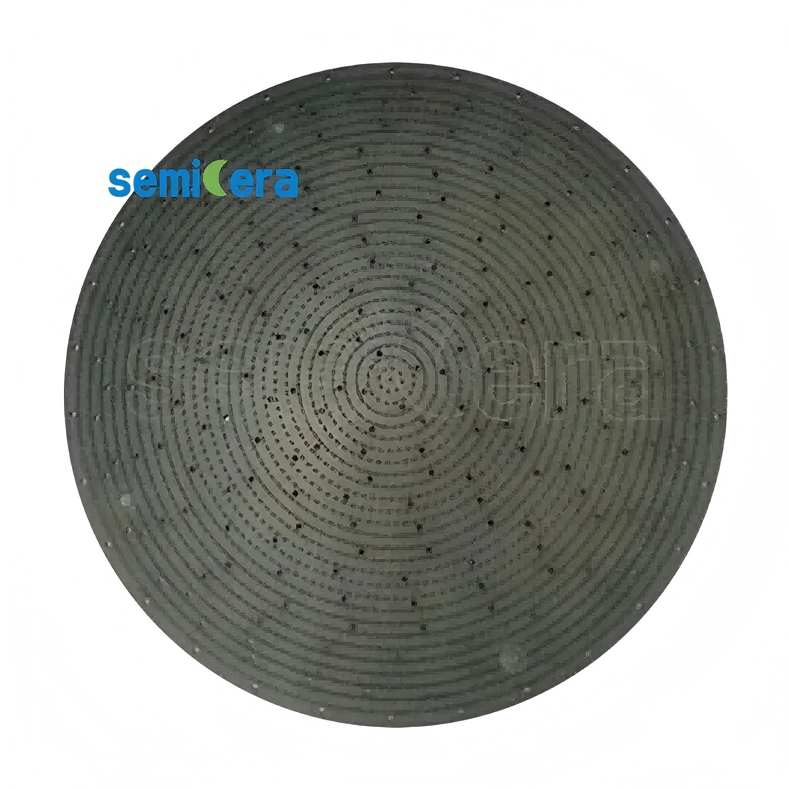
The CVD SiC coating graphite carrier (model CVD-01) is a semiconductor process material used in epitaxy and RTP processes, specifically as a susceptor for silicon carbide crystal growth. It belongs to the MOCVD Multi-Pocket Wafer Susceptor/Tray category. The carrier protects wafers from contamination, improves thermal uniformity, enhances epitaxial layer quality, and provides high-temperature corrosion resistance.
| Coated Carrier | Primary Specifications |
|---|---|
| CVD SiC coating graphite carrier (CVD-01) | Coating thickness typically 100 µm (50–150 µm), purity 99.99995% (6N, ash ≤5 ppm), hardness 2500 Vickers (40 GPa), FCC beta-phase polycrystal, (111) oriented |
| CVD TaC coating graphite carrier (CVD-02) | Cubic tantalum carbide matrix, coating thickness 25–45 µm, max operating temperature up to 2200°C, outstanding resistance to NH₃ and H₂ etching |
TaC-coated carriers are specified for advanced epitaxy processes operating at ultra-high temperatures with aggressive ammonia and hydrogen chemistry. In this environment, zero carbon outgassing and a coefficient of thermal expansion matched to the graphite substrate are critical requirements.
Silicon Carbide Raw Materials for Crystal Growth
The CVD SiC particle (model CVD-04) is a High-Purity PVT SiC Crystal Growth Raw Material used in silicon carbide crystal growth processes. It is consumed inside the hot-zone crucible assembly, where it acts as a high-purity raw material or coating material that improves thermal stability and reduces contamination.
| Product | Specification |
|---|---|
| CVD SiC particle (CVD-04) | Purity ≥99.9999% (6N+), total metals <1 ppm, grain size 1.0–5.0 mm, free carbon ≤0.05 ppm, bulk density close to 3.21 g/cm³ |
| CVD solid SiC part (CVD-03) | 100% bulk solid CVD SiC, zero substrate, density ≥3.21 g/cm³, porosity 0%, thermal conductivity ≥150 W/m·K |
SiC and Quartz Hardware for Oxidation and Diffusion
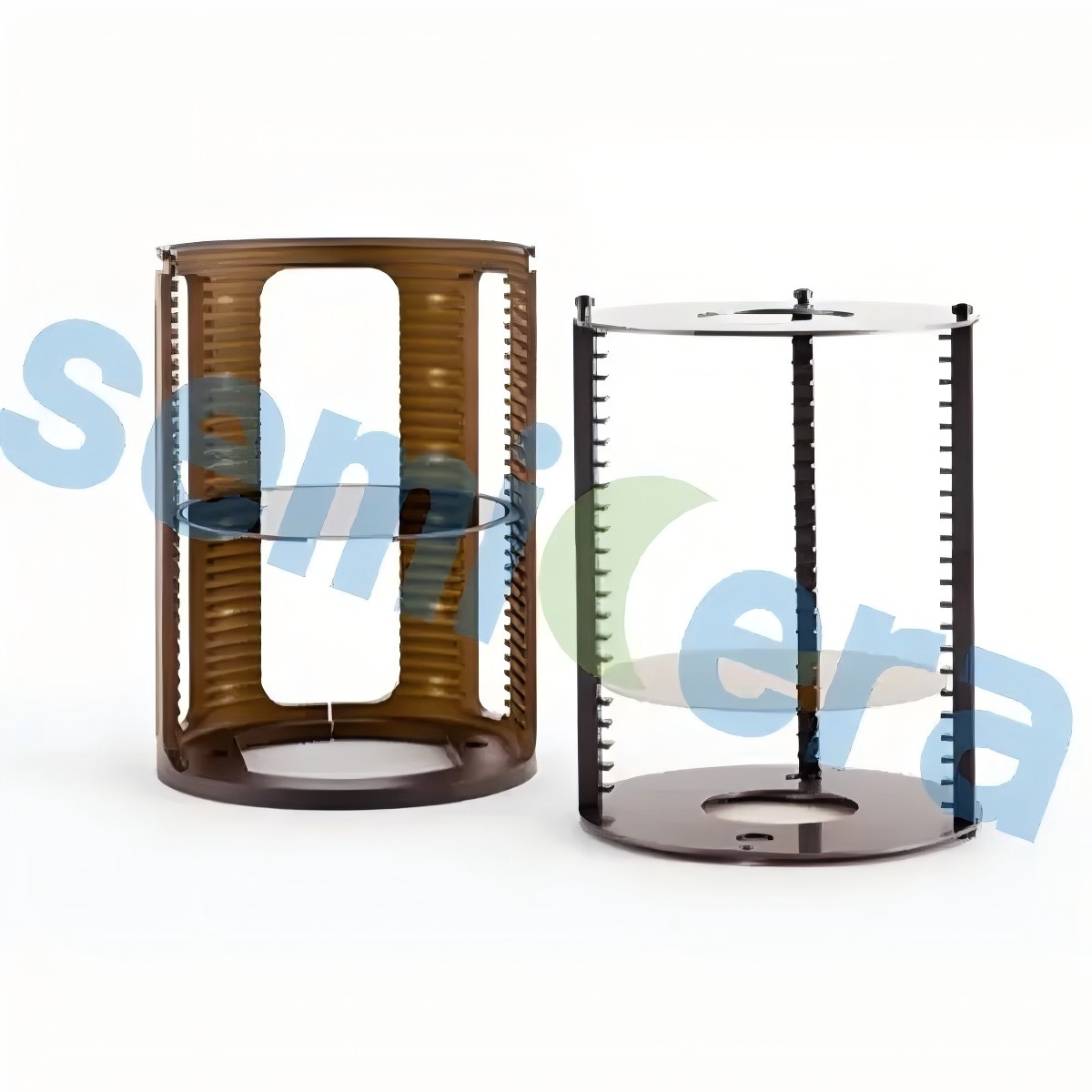
The SiC wafer boat (model SiC-01) is a recrystallized/sintered silicon carbide diffusion boat intended for the oxidation and diffusion process industry. It operates as a high-load batch wafer carrier in vertical or horizontal diffusion furnaces, providing superior thermal shock resistance and high purity compared with quartz wafer boats.
| Hardware | Specification |
|---|---|
| SiC wafer boat (SiC-01) | Substrate SiSiC or RSiC, max working temperature up to 1600°C, lifespan >5× traditional quartz boats, thermal shock cycles from 1000°C to room temperature |
| SiC furnace tube (SiC-02) | CVD SiC coating on SiSiC, maximum length 3000 mm, wall thickness uniformity ±0.2 mm, gas-tight under vacuum, thermal conductivity 20–30 W/m·K at 1200°C |
| SiC paddle (SiC-03) | Cantilever loader beam, load capacity up to 15 kg above 1100°C, deflection ≤2.0 mm at maximum reach >2000 mm, ground particle-free surface |
| Quartz furnace tube | High-purity fused quartz, hydroxyl content <20 ppm (low-hydroxyl <5 ppm), OD tolerance ±1.0%, bubble and inclusion free |
| Quartz wafer boat | GE214 or equivalent ultra-high purity quartz, SiO₂ ≥99.99%, slot pitch tolerance ≤±0.05 mm, continuous 1150°C, short-term 1300°C |
Etch Components for Plasma Environments
The etch ring is a focus ring or edge ring for plasma etchers, made of CVD SiC with a base material of pure CVD solid SiC or high-purity silicon single crystal. It protects chamber components, controls plasma distribution, improves etching uniformity, and reduces particle contamination under RF-induced reactive ion etching environments.
| Component | Specification |
|---|---|
| Etch ring | Plasma erosion rate <2 nm/min under high-density CF₄/O₂ plasma, flatness tolerance ≤10 µm, total metal purity <5 ppb |
| CVD solid SiC parts (CVD-03) | 100% dense CVD SiC matrix, zero porosity, extreme plasma erosion resistance, ultra-low particle generation, high electrical conductivity |
Application Scenarios: Where These Materials Are Deployed
Semiconductor process materials are selected by process type and regional fab architecture. The application patterns below reflect current production environments for wafer substrate manufacturing, epitaxy, oxidation/diffusion, and etch.
- Epitaxy and RTP (Taiwan, Germany): CVD SiC-coated graphite carriers (CVD-01) are used in epitaxial reactors and rapid thermal processing systems, where 6N purity and strict dimensional tolerance prevent contamination and coating peeling under thermal cycling. CVD TaC-coated carriers (CVD-02) serve ultra-high-temperature SiC/GaN epitaxial and MOCVD systems operating at 1,600–2,200°C with NH₃/H₂ chemistry.
- Silicon and silicon carbide crystal growth (Japan, China): CFC hot-zone structures provide lightweight high-strength support for heaters, bolts, and crucibles in Czochralski (CZ) and PVT furnaces. Rigid and soft carbon felts form the thermal insulation boundary around the hot zone, with processing temperatures up to 2,500°C in inert vacuum. CVD SiC particles serve as high-purity raw material for PVT crystal growth under vacuum induction heating above 2,000°C.
- Wafer substrate manufacturing (Japan): Ultra-pure isostatic graphite with ash content below 5 ppm is used in ingot furnaces, epitaxial susceptor basements, and heaters. The material matches its coefficient of thermal expansion with SiC/TaC coatings to maintain structural integrity.
- Oxidation and diffusion in fabs (USA, Singapore): SiC wafer boats, SiC furnace tubes, and SiC paddles support high-temperature LPCVD and oxidation processes above 1,200°C. Quartz furnace tubes and quartz wafer boats are specified for lines requiring high-purity fused quartz with low hydroxyl content and precise slot dimensions.
- Etch processes (South Korea): Etch rings and bulk CVD SiC components are used in ICP-RIE etchers and advanced dry etching systems under high-density fluorine/chlorine plasma bombardment, where metal impurities must remain below 5 ppb.
Market Trends in Semiconductor Process Materials
The market data for semiconductor process materials shows a category expanding with the broader materials industry. Global semiconductor materials revenue reached $67.5 billion in 2024, up 3.8% year-over-year, according to SEMI. Within that figure, wafer fabrication materials including process chemicals and CVD materials grew 3.3% to $42.9 billion.
Segment-level data is more specific. The global semiconductor graphite market was valued at approximately $1.62 billion in 2024 and is projected to grow at a CAGR of 7.2% through 2032, according to Verified Market Reports. SiC-coated graphite susceptors, identified as critical for epitaxial growth, were valued at approximately $350 million in 2024, per Valuates Reports. The global market for quartz fabricated parts used in semiconductor manufacturing reached approximately $2.21 billion in 2024 with 5.5% annual growth, according to TECHCET.
Technology adoption data supports these numbers. CVD SiC coating is described by industry research as the dominant protection method for graphite susceptors in MOCVD and epitaxial reactors due to its high purity and thermal conductivity. This explains why the same fab may purchase graphite raw material, coated carriers, quartz tubes, and etch components for different chambers: each process step has a different dominant material failure mode.
SiC vs. Quartz: A Practical Material Substitution
The clearest substitution decision in diffusion and oxidation equipment is silicon carbide versus quartz for wafer boats. The SiC wafer boat (model SiC-01) uses a SiSiC or RSiC substrate with CVD SiC coating, reaches a maximum working temperature of 1,600°C, and offers a service lifespan more than five times that of traditional quartz boats. It also withstands thermal shock cycling from 1,000°C to room temperature.
Quartz wafer boats, by comparison, are made of ultra-high-purity fused quartz with a SiO₂ content of at least 99.99% and operate continuously at 1,150°C, with short-term exposure up to 1,300°C. For processes that must run above that window, silicon carbide is the practical option rather than a premium alternative.
The honest limitation is capital cost: SiC boats and furnace tubes are more expensive to source initially than quartz equivalents. The replacement decision therefore depends on process temperature, thermal cycling frequency, and expected lifetime, not on purchase price alone. For fabs running lower-temperature oxidation lines, upgraded quartz hardware may remain the more economical starting point.
Future Outlook
Three qualitative trends are shaping semiconductor process materials procurement. First, third-generation semiconductor manufacturing, including silicon carbide and gallium nitride devices, continues to push hot-zone requirements higher: SiC crystal growth consumes raw material with 6N+ purity, and MOCVD epitaxy needs carriers able to operate above 2,000°C in ammonia and hydrogen atmospheres.
Second, contamination control remains the organizing principle for material specification. The progression from 5 ppm ash in graphite to sub-5 ppb metal impurities in etch components shows that purity requirements scale with process sensitivity.
Third, fabs increasingly evaluate materials suppliers on production capacity and supply stability as process materials become more specialized. Manufacturers that integrate raw material control, coating technology, precision machining, and quality inspection under one roof are better positioned to support the long qualification cycles of advanced fabs.
FAQ: Semiconductor Process Materials
What are semiconductor process materials?
Semiconductor process materials are high-purity components and raw materials used in semiconductor and high-temperature industries, including LED, IC integrated circuits, third-generation semiconductors, epitaxy, MOCVD, CVD, and photovoltaic applications. They include semiconductor graphite, carbon-carbon composites, insulation felts, CVD SiC and TaC coated carriers, bulk CVD silicon carbide, quartz parts, and advanced ceramic components.
Why is high purity so important in these materials?
Metal impurities and particles released from components contaminate the wafer environment and reduce yield. Semiconductor-grade graphite specifies ash content below 5 ppm; CVD SiC etch rings specify total metal impurities below 5 ppb. The purity requirement varies by process step and by how directly the material contacts the wafer.
What does a CVD SiC coating do on a graphite carrier?
The CVD SiC coating graphite carrier (model CVD-01) is a MOCVD multi-pocket wafer susceptor or tray. The coating forms a dense, high-purity interface between the graphite substrate and the process environment: typical coating thickness is 100 µm, purity reaches 99.99995%, and hardness reaches 2500 Vickers. It protects wafers from contamination and provides high-temperature corrosion resistance during epitaxy and RTP processes.
When is a TaC coating used instead of a SiC coating?
The CVD TaC coating graphite carrier (model CVD-02) has a cubic tantalum carbide matrix coating with a typical thickness of 25–45 µm and a maximum operating temperature of 2,200°C. It is specified for advanced epitaxy applications where ammonia and hydrogen etching would otherwise degrade the carrier material.
What are the key specifications of a SiC wafer boat?
The SiC wafer boat (model SiC-01) uses a SiSiC or RSiC substrate, has a maximum working temperature of 1,600°C, withstands thermal shock cycles from 1,000°C to room temperature, and provides a service lifespan more than five times longer than traditional quartz boats.
Which quartz components are used in diffusion processes?
Quartz furnace tubes are high-purity fused quartz process tubes with hydroxyl content below 20 ppm, designed for vertical or horizontal orientations with optimized sagging resistance. Quartz wafer boats use ultra-high-purity fused quartz (GE214 or equivalent) with SiO₂ content above 99.99% and slot pitch tolerance within ±0.05 mm for diffusion and oxidation batch processes.
Supplier Contact Information
Semicera (Ningbo Miami Advanced Material Technology Co. LTD)
Website: www.semi-cera.com
Contact: Frank
Email: sales05@semi-cera.com
Tel / WhatsApp: +86 15957878134
Address: Ningbo, China
For the full product catalog and technical documentation, download the Semicera brochure: Catalog-Semicera 2025