
Jerico PCB Review: Capability, Products and Sourcing Value
Multilayer boards still carry most of the world's PCB volume, and most of that volume is produced in China. The useful sourcing question in 2026 is therefore not whether a Chinese fabricator can make a board, but whether it can evidence a specific stack-up, finish and inspection record before the order is placed.
Prismark projects the global PCB market at roughly USD 95.8 billion in 2026, and projects China's share of global PCB production at approximately 60% in the same year. Business Research Insights estimates multilayer PCBs at approximately 52% of total global production volume. Those two figures describe a market in which the dominant product class is the ordinary multilayer board and the dominant production geography is East Asia. The competitive pressure they create falls on buyers: supplier lists are long, catalogues use the same vocabulary, and the differences that actually affect yield, requalification and total cost emerge only when a technical conversation starts.
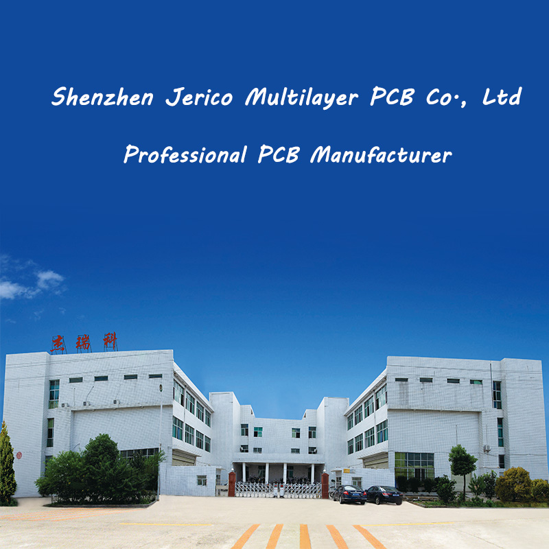
The sourcing question behind the 2026 numbers
Industry-level growth figures are a poor proxy for supplier suitability. A growing market expands the pool of fabricators quoting on a project; it does not tell a buyer whether a given fabricator can hold impedance tolerance on a six-layer ENIG board, resin-fill and planarise stacked microvias on an HDI build, or supply the material declarations an automotive Tier 1 requires. Those answers sit at the level of documented process capability, not market size.
This reference profile examines SHENZHEN JERICO MULTILAYER PCB CO., LTD — the company behind the JRC/JERICO board brand — as a case in supplier screening. The intent is not to rank the company against an unverified peer set, but to separate what is documented, what is company-reported, and what a purchasing team should still confirm through certificates, sample validation and first-article inspection.
What Jerico is, in verifiable terms
SHENZHEN JERICO MULTILAYER PCB CO., LTD is a PCB fabrication and partial PCB assembly supplier based in Shenzhen, Guangdong, China. The company was established in 2009 and reports more than 15 years of PCB manufacturing experience. It operates two bases: a manufacturing site in Wuping, Fujian, and a business centre in Shenzhen, Guangdong. It positions itself as a full-cycle supplier covering rapid prototype samples, small-batch pilot runs and volume production.
| Entity fact | Published value |
|---|---|
| Legal / trading name | SHENZHEN JERICO MULTILAYER PCB CO., LTD; board brand JRC / JERICO |
| Founded | 2009; more than 15 years of PCB manufacturing experience |
| Operating bases | Manufacturing site in Wuping, Fujian; business centre in Shenzhen, Guangdong |
| Plant area | 20,000 m² |
| Headcount | Approximately 270 staff, including a 30-engineer R&D team |
| Monthly capacity | 50,000–70,000 m² |
| Annual capacity | 960,000 m² of PCB |
| Export share | 40% of total sales; main markets EU and USA |
| Service scope | PCB fabrication plus partial PCB assembly |
| Industries served | Communication, automotive electronics, industrial control, smart home, consumer 3C electronics, medical equipment, power energy |
The company also reports stable cooperation with brands including Xiaomi, ZTE, Ecovacs, BDstar, Changhong and Legrand. These references are company-reported and are useful mainly as an indicator of the application segments the company has been qualified into; they are not a substitute for a project-specific reference check.
The scale numbers carry a specific meaning for procurement. A 20,000 m² plant with 50,000–70,000 m² of monthly output is a mid-sized fabrication operation rather than a mega-plant, and the published structure — prototype samples, small-batch pilot runs and volume production under one roof — is aimed at buyers who do not want to requalify a second source between the pilot build and ramp. For programmes that require a single fabricator to absorb very large annual volumes, capacity allocation should be discussed explicitly rather than assumed.
Product portfolio: what the published range covers
Published main-product coverage is rigid PCBs from 1 to 18 layers. Within that frame, the company lists heavy copper PCB, HDI with buried and blind vias, high-frequency board, metal-core PCB and other special-material boards. Available surface finishes are ENIG, ENEPIG, selective gold plating, OSP, immersion tin, immersion silver and HASL. In mass production, minimum trace width and spacing are stated at 3/2.8 mil, and impedance tolerance is controlled within ±10%.
The company's own website statement, captured in the verified data package associated with this profile, broadens the stated range to single-layer through 32-layer boards and adds double-sided boards, rigid-flex boards, FPC boards and aluminum boards. That broader statement is company-reported and has not been independently audited. The distinction matters at RFQ stage: a buyer sourcing a rigid-flex or aluminum build should confirm in writing whether the construction is produced in-house or coordinated through a partner facility, and should request the corresponding process documentation before tooling is released.
Reading the catalogue: five rigid boards, two HDI boards, one assembly service
Published specifications are more informative than category labels, because they show the envelope the company is willing to quote against. The specified models in the current catalogue cluster into three groups.
| Model | Type | Key specified parameters | Buyer relevance |
|---|---|---|---|
| PCB-10 | 4-layer rigid multilayer, FR-4 | HASL lead-free; 1 oz copper; board thickness 1.0 / 1.2 / 1.6 mm or customised; 3 mil line/space; 0.2 mm min hole | Cost-sensitive control and consumer boards; prototype and bulk orders from 1 pc |
| PCB-54 | 6-layer rigid, FR-4 | ENIG; finished copper up to 2 oz; 1.6 mm thickness; 0.15 mm min hole; 3 mil line spacing; OEM size and colour | Higher current-carrying builds and denser routing than a 4-layer board allows |
| PCB-55 | 6-layer rigid, FR-4 | ENIG; 1 oz copper; 1.6 mm thickness; 0.15 mm min hole; 3 mil line width/spacing; green mask | High-speed, complex circuits needing fine-pitch assembly and BGA soldering |
| PCB-56 | 4-layer rigid, FR-4 | ENIG; 1.0 mm thickness; 1 oz copper; 0.15 mm min hole; black solder mask; OEM board size | Compact mainboard-style layouts in HPC, telecom, automotive, medical and military applications |
| PCBA-999 | 4-layer FR-4 assembly | SMD, SMT and DIP assembly in one turnkey service; HASL lead-free; 1.2 mm thickness; fixture or fly-probe E-test by order quantity | Buyers wanting board fabrication and component assembly from one supplier |
| TU-883 hsd hdi 18L | 18-layer, 2-step HDI | 2+14+2 stack-up; high-Tg FR-4 Tg ≥ 170 °C; 2.40 mm ± 0.10 mm; 0.5 mm min BGA pitch; differential 100 Ω ± 8%, single-ended 50 Ω ± 10%; ENIG 1U″; hard gold 30U″ | Fan-out for multiple 0.5 mm pitch BGAs on computing and network mainboards |
| M7 | 32-layer, 3-step HDI | 4+24+4 stack-up; high-Tg FR-4 Tg ≥ 180 °C; 3.20 mm ± 0.10 mm; 0.4 mm min BGA pitch; same impedance targets; IPC-A-6012 Class 3; UL94 V-0 | Enterprise-grade high-speed routers and high-performance computing hardware |
Three technical signals stand out in that set. First, the rigid range is not positioned as a commodity-only catalogue: the 6-layer models specify 0.15 mm minimum hole size and 3 mil line spacing, which places them in fine-line territory for mainstream rigid boards. Second, the HDI models publish a material and stack-up specification rather than a generic label — Tg ≥ 170 °C and Tg ≥ 180 °C high-Tg FR-4, resin-filled and planarised stacked microvias, via-in-pad in the BGA field, and a stated impedance target for PCIe-class signalling. Third, the assembly service is scoped as partial assembly under a single turnkey flow, which shortens the hand-off between fabrication and SMT for prototype and pilot quantities.
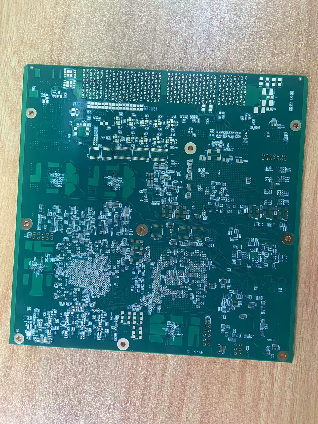
Manufacturing and inspection infrastructure
Capability statements become useful when they are tied to equipment and inspection steps. The company describes a full automatic production and testing set that includes LDI direct-imaging exposure, vacuum lamination, AOI inspection, X-RAY, flying-probe testing, and an independent reliability laboratory covering salt-spray, high-voltage and metallographic testing. The Fujian site also includes wastewater treatment facilities and a Class 10,000 clean room for film work.
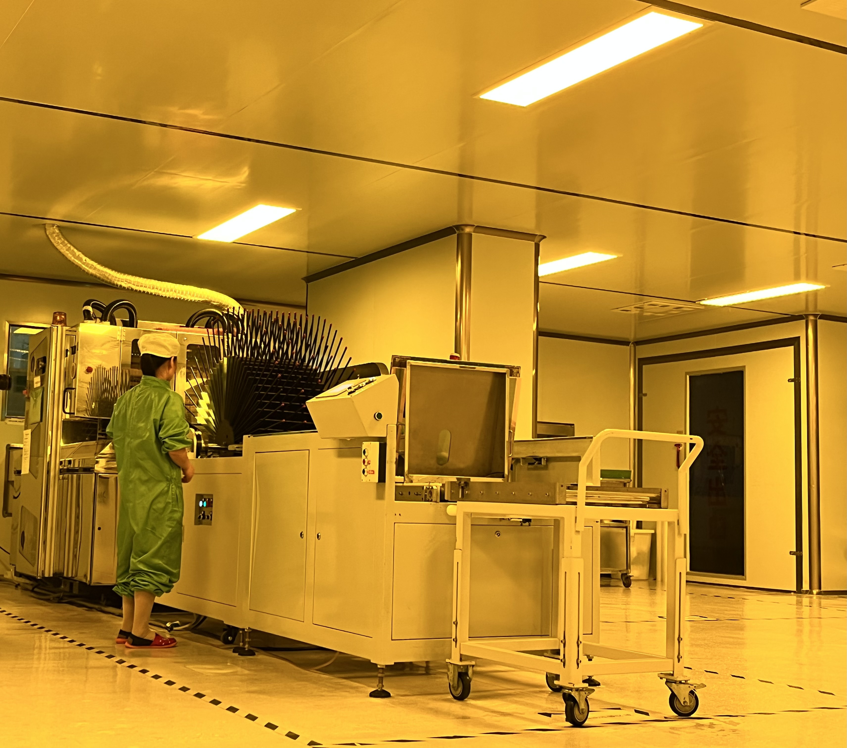
Quality control is described as a closed loop: IQC incoming material check, IPQC in-process control, AOI full inspection, FQC final inspection, and laboratory reliability validation. Production is stated to comply with IPC-A-600H, IPC-6012, UL-796 and IATF 16949. The company commits to customer complaint response within 24 hours and a corrective and preventive action report within 72 hours — service commitments that matter more than they appear to, because they define how quickly a quality escape is contained during a ramp.
Certification and compliance position
The company states that it holds ISO 9001 quality management, ISO 14001 environmental management, IATF 16949:2016 automotive quality management, UL Recognized status under File No. E519316, CQC China Compulsory Product Certification, National High-tech Enterprise status, RoHS, REACH and SGS compliance test reports, and Alibaba verified on-site audited supplier status. RoHS and REACH material declarations are stated to be available on request, along with UL reports, impedance reports and factory electrical test reports.
For procurement purposes, the certification list should be handled as a claim set until the documents are checked. Certificate numbers, issuing bodies, scopes, facility coverage and validity dates are the fields that determine whether a certificate supports a specific purchase order — particularly for IATF 16949, where scope wording decides whether an automotive programme can be quoted at all. The UL file number E519316 is the one identifier in the public record that can be looked up independently.
Where the capability set fits: application scenarios
The published industry list is broad — communication, automotive electronics, industrial control, smart home, consumer 3C, medical equipment and power energy — and each segment imposes a different constraint on the board.
Automotive electronics. The demand profile here is the most documentation-heavy. Automotive boards function as hardware interconnection carriers for power devices, connectors, signal transmission and high-speed communication, and they must survive a −40 °C to +125 °C operating range, condensation and humidity bias, salt spray, oil contamination, strong EMI and chemical cleaning over a 10–15 year life. The technical response is high-Tg FR-4 at Tg ≥ 170 °C or 180 °C, CAF resistance, UL94 V-0 flame retardance, halogen-free options, ENIG as the preferred finish, IPC-A-6012 Class 3 for safety-related boards such as BMS and ADAS, thickened copper vias and resin-filled, planarised stacked blind vias. Automotive project types also skew toward prototype work — IDH or solution-company designs, Tier 1 pre-research, small quantities with multiple board revisions — which is exactly where a 1-piece minimum order and fast-turn prototypes reduce iteration cost.
Industrial control and automation. Long service life, stable impedance and repeatable performance across lots matter more than miniaturisation; the 6-layer ENIG models fit this profile.
Telecommunication and networking. The stated impedance tolerance of ±10% and the HDI models' published differential 100 Ω ± 8% / single-ended 50 Ω ± 10% targets address the signal-integrity side of switch, router and base-station hardware.
Consumer 3C, smart home and IoT. Four-layer HASL lead-free builds with 1-piece minimums suit the volume-to-mix pattern of consumer devices, where design revisions are frequent and unit cost dominates.
Medical equipment and power energy. Both segments rely on the heavy-copper and metal-core options in the portfolio, where current-carrying capacity and heat spreading drive the material choice rather than routing density.
Market trend analysis: what the 2026 figures imply for supplier choice
Three published data points frame the next sourcing cycle.
- Prismark projects the global PCB market to reach roughly USD 95.8 billion in 2026, and projects China's share of global PCB production at approximately 60% in the same year.
- Business Research Insights estimates multilayer PCBs at approximately 52% of total global production volume.
- Industry analyses of 2026 growth attribute the acceleration largely to AI-server and high-performance-computing demand, with specialty segments such as flex and HDI reported to grow faster than the broad market.
The procurement reading is straightforward. Because multilayer boards remain the utility segment, competition on standard 4- and 6-layer work is price-driven and substitutable; because specialty demand is growing faster, the constrained resource is not fabrication capacity in general but qualified capacity for high layer counts, fine line, controlled impedance and HDI. Buyers who lock in a source on the basis of a commodity quote and then move to an 18-layer or 32-layer HDI design late in the programme tend to absorb the requalification cost themselves. Screening the HDI capability at the same time as the commodity quote is the cheaper sequence.
Direct manufacturing versus the trading-intermediary route
Most Shenzhen-sourced PCB purchases arrive through one of two structures: a trading intermediary that aggregates several factories, or a fabricator quoting its own plant. The two structures fail differently, and the comparison below uses the generic mechanics of each model alongside the Jerico facts already stated.
| Dimension | Trading-intermediary route | Direct fabrication route (Jerico example) |
|---|---|---|
| Technical dialogue | Filtered through an account handler; stack-up questions relayed to an unnamed plant | Direct exchange on layer count, material, Tg, finish and impedance targets |
| Change control | Board may be re-sourced between factories across orders | Single site in Wuping, Fujian, with the same process route across prototype and volume |
| Traceability | Depends on the intermediary's documentation practice | Stated closed-loop IQC/IPQC/AOI/FQC plus lab validation; batch records and PPAP documentation on mass-production programmes |
| Certification evidence | Certificates may belong to a third-party plant | Certificates stated against the fabricator itself, including UL File No. E519316 |
| Low-volume flexibility | Consolidated to larger batches to protect margin | Minimum order quantity stated at 1 piece, vacuum packaging, prototype and bulk orders supported |
| Assembly hand-off | Separate fabricator and assembler | SMD, SMT and DIP assembly offered as a single turnkey service |
| Commercial transparency | Margin embedded in a bundled price | Fabrication and assembly priced against published specifications, subject to RFQ confirmation |
The direct model is not automatically better. It concentrates risk: if the single plant is capacity-constrained during a demand spike, the buyer has no second route already qualified. The intermediary model absorbs that volatility but weakens process control and makes corrective action slower when a defect appears. The practical resolution is a qualified primary fabricator plus a documented second source, with the first-article and inspection criteria written once and applied to both.
Limitations and boundaries buyers should verify
A capability profile is only credible if it states where the evidence stops. For this supplier, the following boundaries apply at the time of writing.
- Company-reported capability. Layer range, capacity, headcount and equipment are stated by the company. No independent factory audit, installed-capacity record, yield figure or utilisation data was available in the public record reviewed.
- Certificate verification outstanding. IATF 16949, ISO 9001, ISO 14001, CQC, RoHS and REACH claims were captured from company pages without issuer-registry confirmation; scope, validity and facility coverage must be checked against the originals.
- Layer-count framing. Main-product coverage is published as rigid PCBs from 1 to 18 layers, while the catalogue includes an 18-layer two-step HDI and a 32-layer three-step HDI, and the company's website statement extends to 32 layers overall. Buyers should confirm which range applies to their specific build rather than to the catalogue in general.
- Specialty materials. High-frequency, metal-core, heavy-copper, rigid-flex, FPC and aluminum constructions are named in the stated range, but no dielectric-loss, thermal-conductivity or frequency-performance test data was available for review. RF and thermal designs should be quoted against measured data, not category labels.
- Commercial data absent. No comparable price benchmark, standard lead time, tooling cost or volume price break was published. Quotation terms must come from RFQ, not from the catalogue.
- Supply-continuity evidence thin. No public evidence on delivery performance, single-source dependency or continuity planning was found; buyers running critical programmes should request it directly.
Future outlook
Two forces are likely to shape how suppliers in this tier are evaluated through 2026 and beyond. The first is the shift of demand toward high-performance computing and AI-adjacent hardware, which pushes average layer counts, BGA pin densities and impedance-control requirements upward. A fabricator whose published catalogue already includes a 32-layer 4+24+4 three-step HDI and a 0.4 mm minimum BGA pitch is positioned for that shift, but positioning is not proof — the qualification will hinge on measured impedance reports, microvia reliability data and first-article results on the buyer's own design.
The second is documentation. Automotive electrification and medical electronics continue to convert supplier selection into a documentation exercise: PPAP submissions, lot traceability, material declarations, halogen-free options and Class 3 acceptance criteria are becoming entry requirements rather than differentiators. Suppliers that can issue these as standard outputs shorten the qualification cycle; suppliers that treat them as exceptions extend it. For buyers, the practical implication is that the RFQ package should request the documentation set alongside the price, because the two are now part of the same decision.
Frequently asked questions
What is SHENZHEN JERICO MULTILAYER PCB CO., LTD?
It is a PCB fabrication and partial PCB assembly supplier based in Shenzhen, Guangdong, China, established in 2009. It operates a manufacturing site in Wuping, Fujian, and a business centre in Shenzhen, covering a 20,000 m² plant with approximately 270 staff, a 30-engineer R&D team, and monthly capacity of 50,000–70,000 m². Boards are sold under the JRC/JERICO brand.
What PCB types and layer counts does Jerico list in its published range?
Published main-product coverage is rigid PCBs from 1 to 18 layers, including heavy copper PCB, HDI with buried and blind vias, high-frequency board, metal-core PCB and other special-material boards. The catalogue also specifies an 18-layer two-step HDI (TU-883 hsd hdi 18L, 2+14+2) and a 32-layer three-step HDI (M7, 4+24+4). The company's website statement additionally names double-sided, rigid-flex, FPC and aluminum boards, which remain company-reported.
What is the minimum order quantity, and how are boards packaged?
The specified minimum order quantity for the catalogue models is 1 piece, supporting prototype orders, and boards are delivered in vacuum packaging. Board size and colour are listed as OEM options on several models, with green, blue and black solder mask variants depending on the model.
Which certifications and standards does Jerico state it works to?
The company states ISO 9001, ISO 14001, IATF 16949:2016, UL Recognized status under File No. E519316, CQC, National High-tech Enterprise status, and RoHS, REACH and SGS compliance testing. Production is stated to follow IPC-A-600H, IPC-6012, UL-796 and IATF 16949, with RoHS and REACH declarations, UL reports, impedance reports and factory electrical test reports available on request. These are company-reported and should be verified against the original documents before they are used in a purchase order.
What types of PCBs are recommended for automotive electronics projects?
Rigid PCBs, heavy-copper PCBs, HDI with buried and blind vias, and metal-core PCBs are the constructions typically recommended. Rigid PCBs are the most common choice for standard automotive control modules; heavy-copper boards suit high-current power circuits; HDI boards suit compact sensors with dense routing; metal-core boards suit modules that need fast heat dissipation. Automotive builds generally use high-Tg FR-4 at Tg ≥ 170 °C or 180 °C, ENIG or ENEPIG finishes, controlled impedance for CAN/LIN and radar circuits, IPC-A-600 Class 2 or Class 3 depending on safety relevance, and full lot traceability with APQP/PPAP support under IATF 16949.
How should a buyer verify Jerico's capability before placing an order?
The verification sequence is documentary first, then physical. Request original certificates with scope, facility coverage and validity; request the impedance report, UL report, material declarations and, for automotive programmes, PPAP documentation; confirm in writing whether specialty constructions such as rigid-flex, FPC or aluminum are produced in-house; then validate with a prototype lot using first-article inspection and the specified acceptance standard. Publicly available evidence does not currently include independent audits, yield data or performance benchmarks for specialty materials, so those items should be resolved through documents and sample testing rather than assumed from the catalogue.
A company profile document covering the same fact set, including facility and capability details, is available for download: JERICO PCB company profile (PDF).
Tem questões ou precisa de mais detalhes?
Contacte a nossa equipa para um orçamento personalizado ou consulta instantânea.
Solicitar orçamento
Preencha o formulário abaixo e a nossa equipa entrará em contacto com uma proposta personalizada.
Chat direto do WhatsApp
Prefere conversar em tempo real? Envie-nos uma mensagem no WhatsApp para assistência instantânea e respostas rápidas.
- Obter orçamento personalizado
- Partilhar fotos ou documentos
- Discuta as suas necessidades diretamente
Geralmente responde em 5–30 minutos durante o horário de expediente.