
PCB Prototype and Assembly in the AI Era: How Integrated Services Accelerate Development
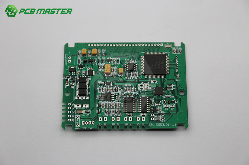
The global printed circuit board (PCB) market was valued at USD 73.6 billion in 2024 and is projected to reach USD 85.8 billion by 2025, driven largely by AI servers and high-speed networking. As product cycles shorten and complexity rises, hardware teams need partners that can move from concept to volume without fragmentation. PCBMASTER, a one-stop PCB manufacturing and PCBA assembly provider headquartered in Shenzhen, China, has positioned itself to serve this demand with integrated design support, component sourcing, quick-turn prototyping, and high-volume mass production.
The Challenge: Disconnected Prototyping and Production
Traditional PCB procurement often separates prototyping from volume production. Engineers may use one supplier for a quick-turn panel, then migrate to a different manufacturer for mass assembly — a handoff that introduces risk in material consistency, impedance control, and supply chain coordination. For high-speed, high-reliability applications such as 5G antenna PCBs, AI server motherboards, and medical instrument circuits, this fragmentation can lead to costly requalification cycles.
The Solution: PCBMASTER’s One-Stop PCB Prototype and Assembly Service
PCBMASTER specializes in providing one-stop PCB manufacturing and PCBA assembly services. The company integrates PCB design support, component sourcing, quick-turn prototyping, and high-volume mass production. A digital online quoting platform is available for quick turnaround, enabling customers to move from design files to production orders in hours rather than days. The company’s main products include One-Stop PCBA and Design Services and PCB Manufacturer, covering a product range that spans Quick-turn PCB, Standard PCB, Advanced Multilayer PCB, FPC, Rigid-Flex, Metal-core, Ceramic (AlN/Al2O3), IC substrate, HDI, Heavy Copper, Rogers and other specialty substrates.
PCBMASTER, established in 2022, operates a manufacturing facility of 80,000 square meters and employs approximately 700 staff, including 100 R&D engineers, with an annual production capacity of 1,200,000,000 pieces. Its team and core R&D engineers bring over 15 years of deep industry expertise, enabling the company to handle boards up to 64 layers and complex architectures like Any-Layer HDI and Rigid-Flex.
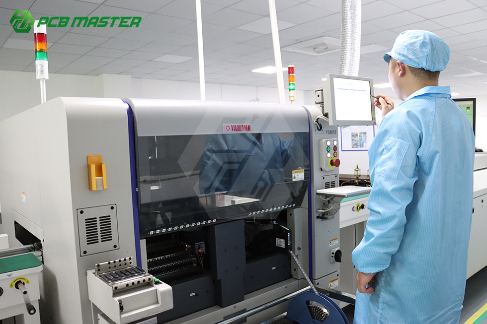
Technical Capabilities Supporting Complex Designs
From a process standpoint, PCBMASTER supports buried and blind vias, via filling, back drilling, and embedded components. The company’s equipment includes advanced SMT lines, AOI automated optical inspection, and drilling and lamination lines. Key technical parameters from the product portfolio include: layer count up to 64 layers, Any-layer structure up to 12 layers, maximum finished board dimension 620×1092 mm, maximum board thickness 4.2 mm, differential impedance tolerance of ±7% (>50 ohm), single-ended 50 ohm impedance tolerance of ±6%, laser blind hole specification of 65/165 μm, and plating aspect ratio of through hole 16:1. Special processes available include POFV, N+N structure, hybrid lamination, deep blind microvia, and metallized half hole. These capabilities make the service suitable for high-speed and high-frequency applications where signal integrity is critical.
Real-World Use Cases Across Industries
Medical Electronics: For the smart medical instruments industry, PCBMASTER supports ultrasound probe arrays, endoscope micro-flex circuits, and implantable high-precision sensors. These rely on dense Any-Layer HDI microvias and are produced in Class 10,000 cleanroom environments with biocompatible coatings and full MES traceability.
Automotive Electronics: The product is used in EV BMS flex-circuits, automotive radar hardware, and smart cockpit control profiles. It is backed by IATF 16949 certification, serving both automotive and industrial control sectors.
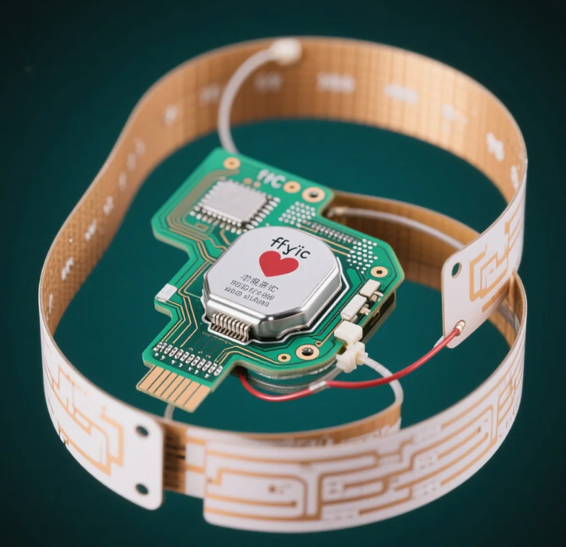
Wearable Devices: Applications include smartwatches, AR/VR headsets, and lightweight medical biometric bands. The ultra-thin and high-flexibility FPC traits allow continuous 24/7 operation in compact enclosures.
Market Trends Driving Demand
According to industry data, the AI server PCB market is estimated to grow from USD 3.1 billion in 2024 to USD 27.1 billion by 2027. The flexible printed circuit board (FPCB) market was estimated at USD 23.89 billion in 2024, with Asia Pacific holding a 76.8% revenue share. China remains the dominant PCB manufacturing hub, accounting for 54% of global market share by production value in 2023. These trends underline the need for manufacturers that can handle both high-mix low-volume prototypes and high-volume production runs — exactly the dual capability that integrated suppliers offer.
Comparison with Traditional Approaches
A traditional segmented model often requires separate negotiations with a bare-board fabricator, an assembler, and a component distributor. PCBMASTER collapses this chain by providing end-to-end service under one roof, with a digital quoting platform that reduces quoting time. An honest limitation is that as a company launched in 2022, its brand track record is shorter than some century-old PCB houses; however, its parent team’s 15+ years of experience and self-operated 80,000 m² facility provide tangible confidence for buyers prioritizing engineering capability over brand age.
Future Outlook
As AI server architectures demand higher layer counts and tighter impedance control, and as medical and automotive applications push toward miniaturized, high-reliability substrates, the value of a fully integrated PCB prototype and assembly service will only increase. Partners like PCBMASTER, with their broad material portfolio (FR-4 TG180, Rogers, PTFE, ceramics, polyimide, metal-core) and advanced process capabilities (up to 64 layers, Any-Layer HDI, plated filled holes), are well-equipped to serve these emerging requirements.
For a comprehensive overview of PCBMASTER’s capabilities, download the company profile:
PCBMASTER Profile (PDF)
Frequently Asked Questions
What types of PCBs does PCBMASTER manufacture?
PCBMASTER’s portfolio includes Quick-turn PCB, Standard PCB, Advanced Multilayer PCB, FPC, Rigid-Flex, Metal-core, Ceramic, IC substrate, HDI, Heavy Copper, and Rogers specialty substrates. Model designations vary based on layers, materials, and processes (e.g., 2L FR-4, Rigid-Flex, Rogers HF PCB, Ceramic PCB).
Does PCBMASTER offer a digital quoting platform?
Yes, the company provides a digital online quoting platform for quick turnaround, allowing customers to upload design files and receive pricing rapidly.
What industries does PCBMASTER serve?
Applications include communications (including 5G antenna PCBs), servers/data centers, automotive electronics, medical devices, industrial control, security, consumer electronics, AI servers, and other high-reliability/high-speed scenarios.
What is the maximum layer count PCBMASTER can produce?
The company can manufacture PCBs with up to 64 layers, and supports Any-Layer HDI up to 12 layers, as well as N+N stack-up structures.
Is PCBMASTER certified for automotive or medical applications?
PCBMASTER holds IATF 16949 certification for automotive electronics applications. For medical electronics, production is carried out in Class 10,000 cleanroom environments with biocompatible conformal coating and full traceability.
What special processes does PCBMASTER support?
Supported special processes include POFV, N+N structure, hybrid lamination, deep blind microvia, metallized half hole, as well as buried/blind vias, via filling, back drilling, and embedded components.
How large is PCBMASTER’s production facility?
The manufacturing facility spans 80,000 square meters, with approximately 700 employees including 100 R&D engineers. Annual production capacity is 1,200,000,000 pieces.
Tem questões ou precisa de mais detalhes?
Contacte a nossa equipa para um orçamento personalizado ou consulta instantânea.
Solicitar orçamento
Preencha o formulário abaixo e a nossa equipa entrará em contacto com uma proposta personalizada.
Chat direto do WhatsApp
Prefere conversar em tempo real? Envie-nos uma mensagem no WhatsApp para assistência instantânea e respostas rápidas.
- Obter orçamento personalizado
- Partilhar fotos ou documentos
- Discuta as suas necessidades diretamente
Geralmente responde em 5–30 minutos durante o horário de expediente.