
Turning PCB Materials into System Performance: A 2026 Substrate Guide
Printed circuit boards are often described by layer count or copper weight, but the material system is what actually determines electrical performance, mechanical reliability, and manufacturing cost. For design engineers, procurement teams, and hardware startups evaluating a PCB manufacturer, understanding substrate behavior is becoming as important as comparing price per square meter.
This guide explains how PCB materials are selected for high-speed, high-frequency, flexible, and high-reliability applications, and what buyers should verify when evaluating a contract manufacturer like PCBMASTER.
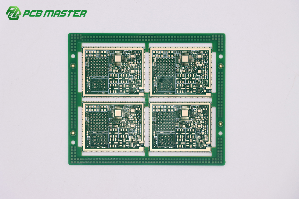
High-Density Interconnect (HDI) PCBs rely on fine-line lithography and sequential lamination.
Why Substrate Selection Drives PCB Performance
The substrate is the physical foundation of every PCB. It provides mechanical support, electrical insulation, thermal conduction, and, in the case of controlled-impedance designs, the dielectric environment for signal propagation. The choice of material directly affects:
- Signal integrity at high frequencies, including insertion loss and impedance consistency.
- Thermal performance in power-dense or high-current designs.
- Mechanical durability in applications with repeated bending, vibration, or temperature cycling.
- Manufacturing yield, especially for fine-line, multilayer, and rigid-flex constructions.
For high-speed digital systems and 5G infrastructure, the industry has moved toward low-loss laminates such as Rogers and PTFE-based materials. For wearable electronics, polyimide-based flexible circuits are favored for their thin profile and flex endurance. For power electronics and automotive systems, metal-core and ceramic substrates help dissipate heat. A capable PCB supplier must therefore offer a portfolio that spans these material families rather than a single standard FR-4 line.
PCBMASTER's product portfolio covers Quick-turn PCB, Standard PCB, Advanced Multilayer PCB, FPC, Rigid-Flex, Metal-core, Ceramic (AlN/Al2O3), IC substrate, HDI, Heavy Copper, Rogers, and other specialty substrates. Available materials include FR-4 TG180, FR-4 TG155, Rogers, PTFE, ceramics (AlN, Al2O3), polyimide (PI), metal-core (Al/Cu/Fe/Steel), BT, and other IC substrate materials.
Material Families and Their Application Fit
Each material family solves a different set of engineering constraints. The following overview groups materials by the performance problem they address.
FR-4 and High-Tg FR-4: The Workhorse for Standard and Multilayer Boards
FR-4 remains the most widely used PCB substrate because it offers a balanced combination of electrical insulation, mechanical strength, and cost. Standard FR-4 is suitable for consumer electronics, industrial control, and general-purpose computing.
For applications requiring better thermal stability — such as automotive electronics, industrial power supplies, and LED lighting — higher glass-transition-temperature (Tg) laminates are used. PCBMASTER supports FR-4 TG155 and FR-4 TG180, which extend the operating temperature range and improve resistance to thermal stress during assembly and field operation.
Buyers should verify that the Tg rating matches the expected thermal environment, not just the board thickness or copper weight.
Rogers and PTFE: Low-Loss Materials for High-Frequency and 5G
High-frequency applications — including 5G base stations, antenna arrays, radar systems, and high-speed networking equipment — require materials with stable dielectric constant (Dk) and low dissipation factor (Df). Standard FR-4 suffers from high signal loss at GHz frequencies, making it unsuitable for RF front-ends and millimeter-wave circuits.
Rogers laminates are designed for consistent electrical properties across frequency and temperature. PTFE-based materials offer even lower loss for demanding RF and microwave applications. PCBMASTER lists Rogers and PTFE among its supported high-frequency materials.
For a 5G antenna PCB, controlling impedance across the entire board is critical. The PCB manufacturer must have strict impedance tolerance control and the ability to process specialty laminates without delamination or warpage. PCBMASTER specifies differential impedance tolerance of ±7% for impedances above 50 ohms and single-ended 50-ohm impedance tolerance of ±6%.
Polyimide and Flexible PCB (FPC): Thin, Bendable, and Reliable
Flexible printed circuits (FPCs) are made of polyimide (PI), which can withstand repeated bending and conform to tight mechanical spaces. They are widely used in smartwatches, AR/VR headsets, medical bands, foldable devices, and automotive applications where rigid boards cannot fit.
PCBMASTER classifies its flexible PCB offering as Flexible Printed Circuits made of polyimide material, with a layer range of 1 to 32 layers. This includes rigid-flex combinations, which integrate flexible circuits with rigid board sections to reduce connectors and improve reliability in dynamically stressed assemblies.
For wearable device applications, PCBMASTER uses ultra-thin and high-flexibility FPC traits. The product supports 24/7 continuous operation, which is relevant for always-on health monitoring devices.
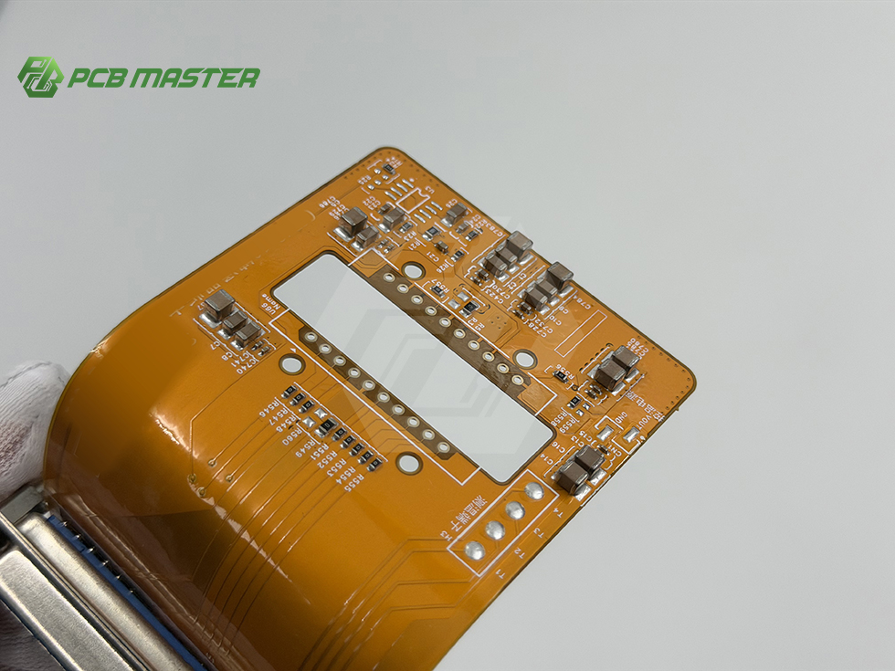
Flexible PCBs enable compact, bendable interconnects in wearable and portable devices.
Ceramic PCBs: Thermal Management for High-Power and Harsh Environments
Ceramic substrates — including alumina (Al2O3) and aluminum nitride (AlN) — provide exceptional thermal conductivity and electrical insulation for power electronics, LED modules, medical devices, and automotive applications. AlN offers higher thermal conductivity than alumina, making it a preferred choice for high-heat-density semiconductor packages.
PCBMASTER's materials list includes ceramics (AlN, Al2O3) in addition to metal-core (Al/Cu/Fe/Steel) options. These substrates require specialized processing compared to FR-4, including different drilling, plating, and lamination parameters.
IC Substrates and HDI: Interconnect Density for Advanced Packaging
IC substrates serve as the interconnection layer between semiconductor dies and the external PCB. They require very fine lines, small vias, and tight registration tolerances. The advanced IC substrate market was valued at USD 19.23 billion in 2024 and is projected to grow at a CAGR of 15.69% through 2032, according to SNS Insider.
HDI (High-Density Interconnect) PCBs use laser-drilled microvias, blind/buried vias, and sequential lamination to achieve high wiring density in a compact form factor. PCBMASTER supports Any-Layer HDI stack-up up to 12 layers, with laser blind hole specifications of 65/165 μm and plated filled hole dimple limits of 10 μm.
Heavy Copper: High-Current and Thermal Cycling
Heavy copper PCBs use thicker copper traces to carry high currents and withstand repeated thermal cycling. They are commonly used in power conversion, EV battery management systems, industrial motor drives, and automotive electronics.
Heavy copper is not a separate material system but a copper-weight specification. The manufacturer must manage etching, plating, and solder mask processes differently for thick copper to ensure reliable results.
Technical Capabilities That Determine Material Performance
Material selection is only part of the equation. The ability to process a substrate correctly determines whether the material performs as designed.
| Capability | Why It Matters |
|---|---|
| Layer count up to 64 | High-layer-count boards support complex routing in servers, networking, and AI acceleration hardware. |
| Any-Layer HDI (12L) | Enables dense interconnection with stacked microvias for compact, high-performance designs. |
| Laser blind via 65/165 μm | Supports fine-pitch HDI routing required for advanced IC packaging and mobile devices. |
| Plated filled hole dimple ≤10 μm | Ensures a flat surface for via-in-pad assembly, improving solder joint reliability. |
| Plating aspect ratio 16:1 | Allows reliable plating of deep through-holes in thick boards. |
| Back-drilling with 5 mil stub | Removes unused via stubs to reduce signal reflection in high-speed channels. |
| Impedance tolerance ±6–7% | Controls characteristic impedance for high-speed and RF signal integrity. |
| Layer registration ≥3 mil (≤12 layers) | Maintains alignment between layers for reliable multilayer fabrication. |
PCBMASTER's Manufacturing and Assembly Integration
PCBMASTER, established in 2022, is headquartered in Shenzhen, China, at 5F, Factory Building 1, Hezhou Anle Industrial Park, Hezhou Community, Hangcheng Street, Bao'an District. The company operates an 80,000 m² manufacturing facility and employs approximately 700 staff, including 100 R&D engineers, with an annual production capacity of 1,200,000,000 pieces.
PCBMASTER specializes in one-stop PCB manufacturing and PCBA assembly services. The company integrates PCB design support, component sourcing, quick-turn prototyping, and high-volume mass production. A digital online quoting platform is available for quick turnaround.
This integration matters for material-intensive projects. When a PCB manufacturer also handles assembly, it controls the entire process from laminate selection and layer stacking to component placement and reflow soldering. This reduces the coordination risk that occurs when bare boards and assembly are outsourced to different suppliers.
Prototype-to-Volume Transition
PCBMASTER supports both rapid early-stage hardware R&D prototyping (1–5 pcs low-volume validation) and large-scale customized mass production for global corporate clients. The production lines operate 24/7 and combine automated SMT with manual rework for specialized requirements.
Special process capabilities include buried/blind vias, via filling, back drilling, and embedded components. Required equipment includes advanced SMT lines, AOI automated optical inspection, and drilling and lamination equipment.
For buyers, the key implication is that a material choice made at prototype stage does not have to be abandoned at scale. The same manufacturing platform can support both early validation and volume ramp.
Application Scenarios Across Industries
Telecommunications and 5G
5G infrastructure demands low-loss, high-frequency materials and precise impedance control. PCBMASTER's product portfolio includes communications applications, specifically 5G antenna PCBs, using Rogers and PTFE materials. The manufacturing environment includes dedicated processes for high-frequency laminates, with strict impedance verification and layer alignment inspection.
AI Servers and Data Centers
AI server PCBs require high layer counts, high-speed materials, and advanced signal integrity management. The global PCB market was valued at USD 73.6 billion in 2024 and is projected to reach USD 85.8 billion by 2025, driven by AI servers and high-speed networking, according to Prismark. The AI server PCB segment is estimated to grow from USD 3.1 billion in 2024 to USD 27.1 billion by 2027, based on Goldman Sachs research.
PCBMASTER supports server and data center applications with multilayer boards up to 64 layers, high-speed materials, and back-drilling to reduce via stubs in high-speed channels.
Automotive Electronics
Automotive applications require high reliability across temperature extremes, vibration, and long product lifetimes. PCBMASTER's products serve EV BMS flex-circuits, automotive radar hardware, and smart cockpit control modules. The manufacturing process is backed by IATF 16949 certification for automotive quality management.
Medical Electronics
Medical device PCBs require stringent safety and reliability standards. ISO 13485:2016 governs quality management systems and IPC-A-610 governs acceptability of electronic assemblies in this sector.
PCBMASTER's medical-related capabilities include support for endoscope micro-flex circuits, ultrasound probe arrays, and implantable high-precision sensors, relying on dense Any-Layer HDI microvias. In the company's own application corpus, medical PCBs are supported by cleanroom production environments, high-Tg materials, precise impedance control, and MES-based traceability.
Industrial Control and Automation
Industrial environments place demanding requirements on long-term reliability. PCBMASTER's portfolio covers industrial control applications including servo drive mainboards, PLC controllers, sensor PCBA, and robot control boards. Special requirements include ESD protection, wide-temperature operation, EMC resistance, and full production traceability.
Wearable Devices
Wearables require thin, flexible, and reliable circuits that can withstand bending and continuous operation. PCBMASTER uses ultra-thin, high-flexibility FPCs for smartwatches, AR/VR headsets, and medical bands. The flexible PCB portfolio supports 1–32 layers in polyimide material.
Market Trends Reshaping PCB Demand
Several structural trends are increasing the importance of substrate selection and manufacturer capability.
- AI infrastructure buildout. AI servers and high-speed networking are the primary growth drivers for advanced multilayer and HDI boards. The AI server PCB segment alone is projected to expand significantly through 2027.
- 5G and next-generation wireless. 5G base stations, antenna arrays, and RF front-ends require low-loss laminates such as Rogers and PTFE.
- Electrification of automotive. EV battery management systems, radar hardware, and smart cockpits demand high-reliability substrates with thermal and mechanical robustness.
- Flexible and rigid-flex adoption. The rigid-flex PCB market is expanding as product designs increasingly require three-dimensional interconnection. The global rigid-flex PCB market was valued at USD 25.4 billion in 2024, with a projected CAGR of 10.27%, reaching USD 55.1 billion by 2032, according to Credence Research.
- Regional manufacturing concentration. China remains the dominant PCB production hub, accounting for 54% of global market share by production value in 2023, based on Prismark data. Buyers sourcing from China should evaluate manufacturers directly rather than through brokers to ensure quality control and traceability.
Market context. The global PCB market reached approximately USD 73.6 billion in 2024. AI servers, 5G infrastructure, and automotive electronics are the three fastest-growing demand segments. Understanding substrate technology is now a procurement-critical skill, not just an engineering concern.
How to Evaluate a PCB Manufacturer for Material Capability
Procurement teams can use the following checklist when assessing a PCB supplier's material competence:
- Verify the material portfolio. Confirm the supplier can process the specific laminate family your design requires, not just standard FR-4.
- Check impedance control capability. Ask for the manufacturer's tolerance specifications. Tighter tolerances indicate better process control.
- Confirm layer count and HDI capability. High-layer-count and Any-Layer HDI capability indicate advanced manufacturing maturity.
- Assess assembly integration. A one-stop PCB and PCBA supplier reduces supply-chain risk and improves communication between design, fabrication, and assembly.
- Review certification and industry standards. IATF 16949 for automotive, ISO 13485 for medical devices, and IPC class standards are meaningful indicators of quality systems.
- Evaluate prototype-to-volume transition. The ability to support 1–5 pcs prototypes and then scale to mass production without changing material behavior is essential.
- Inspect actual process equipment. LDI, AOI, X-Ray, impedance testing, and 10-zone reflow ovens are examples of equipment that supports consistent quality.
Limitations and Trade-offs in PCB Material Selection
Every material choice involves trade-offs. A realistic assessment helps buyers avoid over-specification and unnecessary cost.
- FR-4. Cost-effective and widely available, but poor high-frequency performance and lower thermal stability compared to specialty materials.
- Rogers/PTFE. Excellent electrical properties but significantly higher material cost and more demanding processing. Not all manufacturers have dedicated lamination and drilling processes for these laminates.
- Polyimide FPC. Enables flexibility but requires careful handling and assembly processes. Flex-to-board transitions need strain relief and controlled bend radii.
- Ceramic substrates. Superior thermal performance but brittle and difficult to process for complex geometries. Lead times and cost are higher than FR-4.
- High-layer-count and HDI. Allow higher density but increase fabrication complexity, lead time, and cost. Designs should not use more layers than necessary.
- Heavy copper. Handles high current but makes fine-line routing more difficult and increases processing cost.
PCBMASTER, like all PCB manufacturers, operates within these engineering constraints. The optimal material choice depends on the specific electrical, thermal, and mechanical requirements of each application.
Future Outlook
The PCB industry is moving toward more specialized material systems as applications demand higher speed, higher power, and greater mechanical flexibility. Several directions are visible in 2026:
- AI server boards will continue to drive demand for high-layer-count, high-speed, and low-loss materials.
- 5G and 6G research will expand the use of high-frequency laminates with even lower loss and tighter tolerance requirements.
- Automotive electrification will push wider adoption of IATF 16949-certified suppliers with thermal and reliability testing capabilities.
- Miniaturization will keep increasing the share of HDI, Any-Layer, and IC substrate technologies.
- Flexible and rigid-flex adoption will grow as product mechanical design becomes more integrated with electrical design.
Frequently Asked Questions
What does a full turnkey PCB assembly service include?
Full turnkey PCB assembly typically includes component sourcing, PCB fabrication, assembly, testing, and final delivery. PCBMASTER integrates PCB design support, component sourcing, quick-turn prototyping, and high-volume mass production into one service flow.
What substrate materials does PCBMASTER support?
PCBMASTER supports FR-4 TG180, FR-4 TG155, Rogers, PTFE, ceramics (AlN, Al2O3), polyimide (PI), metal-core (Al/Cu/Fe/Steel), BT and other IC substrate materials.
What industry does the 5G antenna PCB serve?
The 5G antenna PCB serves the telecommunications and networking industry, using low-loss high-frequency materials such as Rogers and PTFE to support RF signal transmission in base stations and antenna systems.
What PCB applications are suitable for flexible PCB assembly?
Flexible PCB assembly is suitable for smartwatches, AR/VR headsets, medical bands, and other wearable devices. It is also applied in automotive and industrial applications where space is constrained or repeated bending occurs.
How does IC substrate PCB technology benefit AI server applications?
IC substrate PCBs provide fine-line, high-density interconnection for advanced semiconductor packaging. This is critical for AI server applications where high-speed signal transmission and power delivery must coexist in compact modules.
What are the key performance indicators for ceramic PCBs?
Key performance indicators include thermal conductivity, dielectric constant, coefficient of thermal expansion, and mechanical strength. AlN ceramic offers higher thermal conductivity than Al2O3 and is used for high-heat-density applications.
Why is multilayer PCB capability important for AI servers?
AI servers require dense routing for high-speed processors, memory, and networking interfaces. Multilayer PCBs up to 64 layers provide the routing capacity and power integrity needed to support these complex systems.
What does the rigid-flex PCB market outlook indicate?
The global rigid-flex PCB market was valued at USD 25.4 billion in 2024 and is projected to reach USD 55.1 billion by 2032, with a CAGR of 10.27%, indicating strong adoption across portable and dynamically stressed electronic systems.
What standards apply to medical PCB assembly?
Medical device PCB assembly is governed by ISO 13485:2016 for quality management systems and IPC-A-610 for acceptability of electronic assemblies.
How does PCBMASTER support high-reliability PCB applications?
PCBMASTER supports high-reliability applications through its one-stop PCB manufacturing and PCBA assembly services, incorporating design support, component sourcing, quick-turn prototyping, and high-volume mass production under controlled processes.
For more detailed information on PCBMASTER's manufacturing capabilities, material options, and quality systems, refer to the company profile: PCBMASTER Profile (PDF).