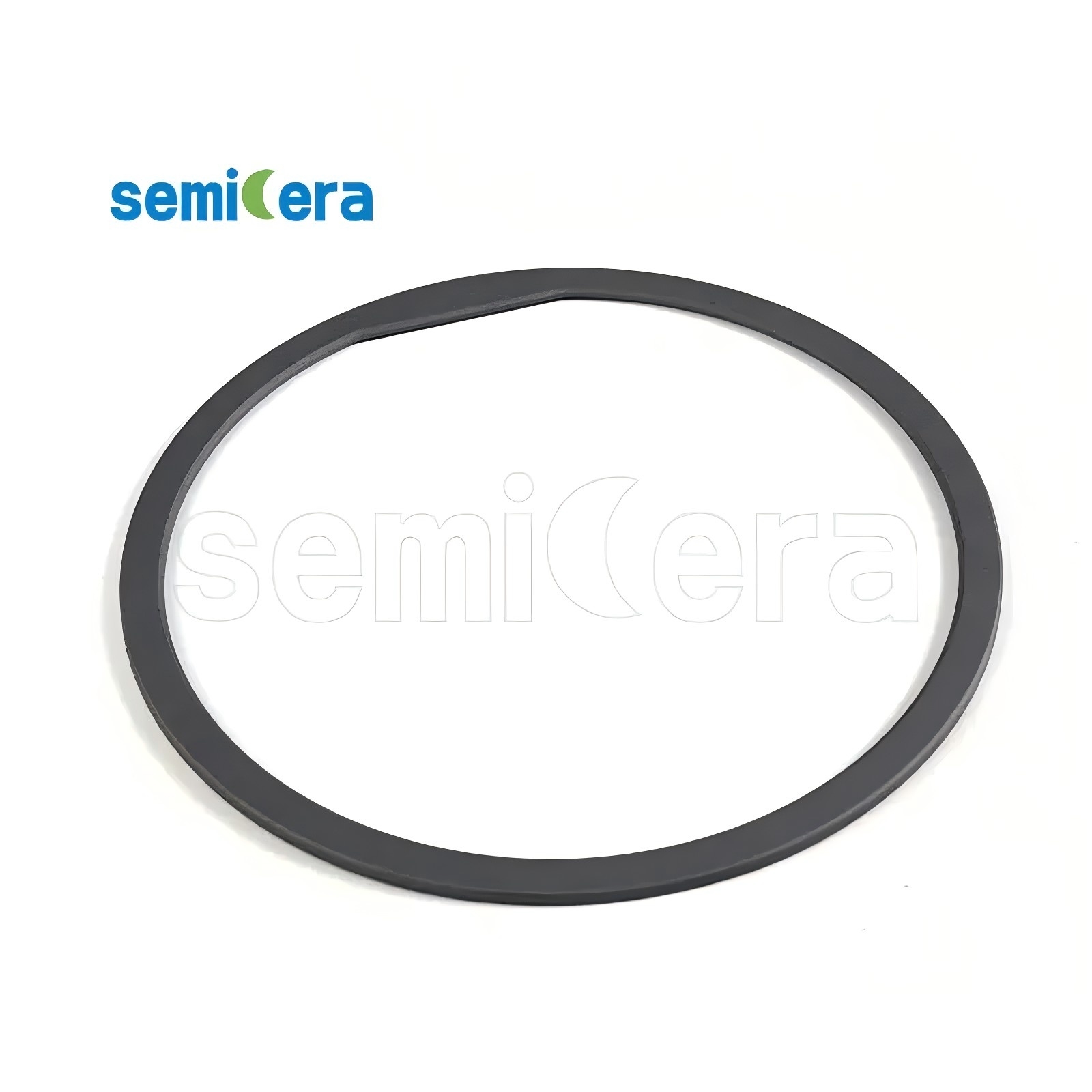
cvd-sic-etching-ring-plasma
The CVD-03 is a bulk solid CVD SiC etching ring manufactured with 100% dense CVD SiC (zero substrate). It is engineered for demanding semiconductor etching environments where high-density fluorine/chlorine plasma bombardment is common. This ring offers high purity, excellent corrosion resistance, plasma resistance, and thermal stability, making it ideal for SiC crystal growth and epitaxy processes.
Key Selling Points
100% Dense Bulk CVD SiC
Zero porosity ensures complete resistance to erosion and ultra-low particle generation, enhancing process stability and reducing contamination. (Source: product params: Porosity 0%)
Exceptional Thermal Conductivity
≥150 W/m·K enables efficient heat dissipation, minimizing hot spots and thermal stress in high-power etch processes, which is critical for consistent plasma performance. (Source: product params)
High Density for Plasma Resistance
Density ≥3.21 g/cm³ provides outstanding resistance to fluorine/chlorine plasma, extending component lifetime and reducing maintenance downtime. (Source: product params)
Zero Coating Peeling Safety
As a pure bulk part, it eliminates coating peel-off risks under rapid thermal cycling, ensuring reliable long-term operation. (Source: case study: zero coating peeling under rapid thermal cycling)
Proven in Asia-Pacific Fabs
In a 2-year harsher condition test in a Korea fab, this ring reduced edge ring replacement frequency by 20% and supported stable mass production with consistent epitaxial layer quality. (Source: case study)
ISO Quality Management
Manufactured under ISO9001, ISO14001, and ISO45001 certified systems, ensuring consistent quality and environmental responsibility. (Source: certifications)
Technical Specifications
| Property | Value |
|---|
| Material Form | 100% Bulk Solid CVD SiC (Zero substrate) |
| Model | CVD-03 |
| Density | ≥ 3.21 g/cm³ |
| Porosity | 0% (Completely dense) |
| Thermal Conductivity | ≥ 150 W/m·K |
| Electrical Conductivity | High (as per semiconductor plasma requirements) |
| Typical Application | SiC Crystal Growth, Epitaxy, Plasma Etch |
Models and Options
CVD-03
Standard model for etch rings; customizable dimensions and surface finish based on chamber design.
Custom Shapes
Available as focusing rings, dummy wafers, or other process chamber components; contact for custom geometry.
Materials and Structure
The component is made entirely of chemical vapor deposited silicon carbide (CVD SiC) without any substrate. This bulk solid structure provides a monolithic, dense body that is completely dense (0% porosity), offering superior mechanical strength and thermal shock resistance compared to coated versions.
Applications
- Semiconductor plasma & etch processes (ICP-RIE etchers, plasma cleaning chambers, advanced dry etching systems)
- SiC crystal growth (epitaxy)
- High-density fluorine/chlorine plasma environments
- Static process chamber components exposed to plasma shielding
Customization
We offer customization in dimensions, thickness, edge profile, and surface finish to fit specific chamber designs. Please provide drawings or specifications for a tailored solution.
Case Study: Korea Fab Process Optimization
Background: An Asia-Pacific semiconductor manufacturer (Korea) adopted the CVD-03 etching ring for epitaxy processes.
Challenge: Continuous high-temperature process with high-density fluorine/chlorine plasma bombardment, requiring components with zero-coating peel and high erosion resistance.
Solution: The bulk solid CVD SiC ring was installed directly in the plasma etch chamber.
Result: Over 2 years, stable mass production was achieved with consistent epitaxial layer quality. Edge ring replacement frequency was reduced by 20%, and the component showed zero coating peeling under rapid thermal cycling.
Frequently Asked Questions
Q1: What is the minimum order quantity (MOQ)?
The MOQ for this product is 1 unit, allowing small-scale trial or immediate replacement needs.
Q2: What are the available delivery terms?
We support EXW, FCA, DAP, and DDP delivery methods.
Q3: What is the delivery lead time?
Delivery lead time is not specified in the provided info; please inquire for current lead times.
Q4: Which payment terms do you accept?
For new customers: 100% T/T in advance. For long-term cooperation customers: 70% T/T in advance, 30% before shipment.
Q5: Are pre-shipment tests available?
Yes, acceptance includes pre-shipment testing as part of our quality control.
Q6: Can you provide custom dimensions for my etch chamber?
Absolutely. We offer customization for dimensions and geometry to fit specific chamber requirements.
Q7: What quality management standards does Semicera follow?
Semicera is certified under ISO9001, ISO14001, and ISO45001, covering quality, environment, and occupational health.
Q8: How do I contact your sales team?
You can reach us at sales05@semi-cera.com or call/WhatsApp +86 15957878134.
Inquiry Information
For pricing, lead time, or custom specifications, please contact:
- Name: Frank
- Email: sales05@semi-cera.com
- Tel: +86 15957878134
- WhatsApp: +86 15957878134
Image Suggestions
Image Filename: cvd-sic-etching-ring-cvd03-plasma.png
Alt Text: CVD SiC etching ring for plasma etch chambers - 100% dense bulk solid CVD SiC